2010
Symposium on VLSI Technology Contact
Information:
Hilton Hawaiian Village VLSI
Secretariat USA
2005 Kalia
Road 301-527-0900
ext. 2
Honolulu, Hawaii 96815-1999 vlsi@vlsisymposium.org
808-949-4321
The
following press materials may be downloaded from this site for pre-conference
publicity.
Selected
images from the abstracts are presented in two formats:
-
Word file with
images associated with a highlighted paper and the caption (click on the title)
-
JPE file with
individual, high-resolution images
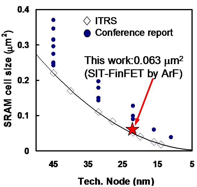
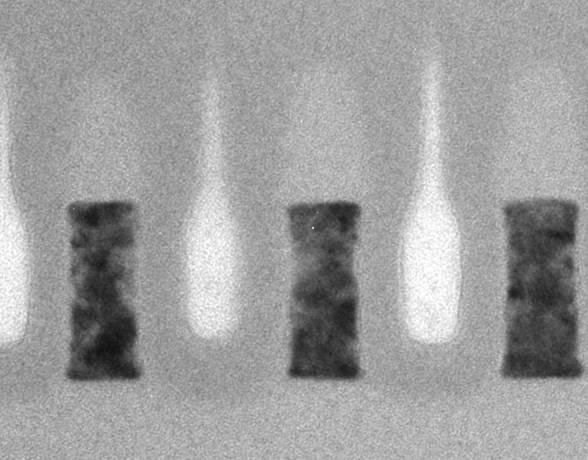
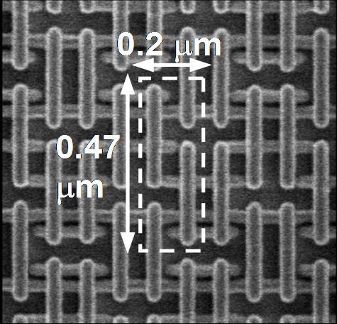
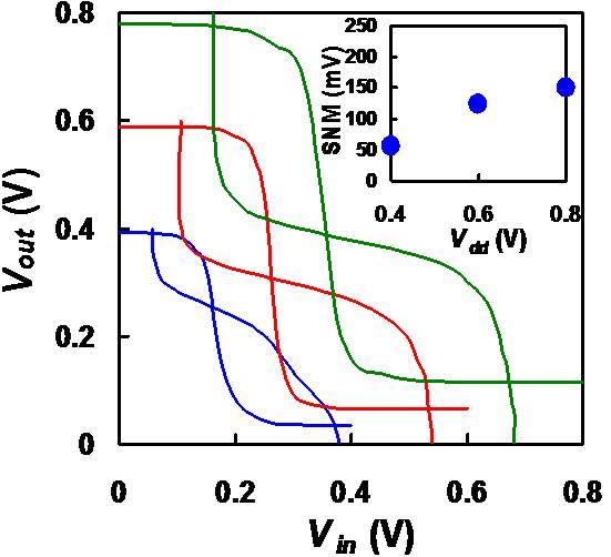
2.2 “A 0.063 μm2 FinFET
SRAM cell demonstration with conventional lithography using a novel integration
scheme with aggressively scaled fin and gate pitch,” V. Basker, et al., IBM
Research, GLOBALFOUNDRIES Inc., Toshiba Corp., NEC Electronics & Albany Nano Tech
High Resolution Images
2.2 Figure 1
2.2 Figure 4
2.2 Figure 6
2.2 Figure 16
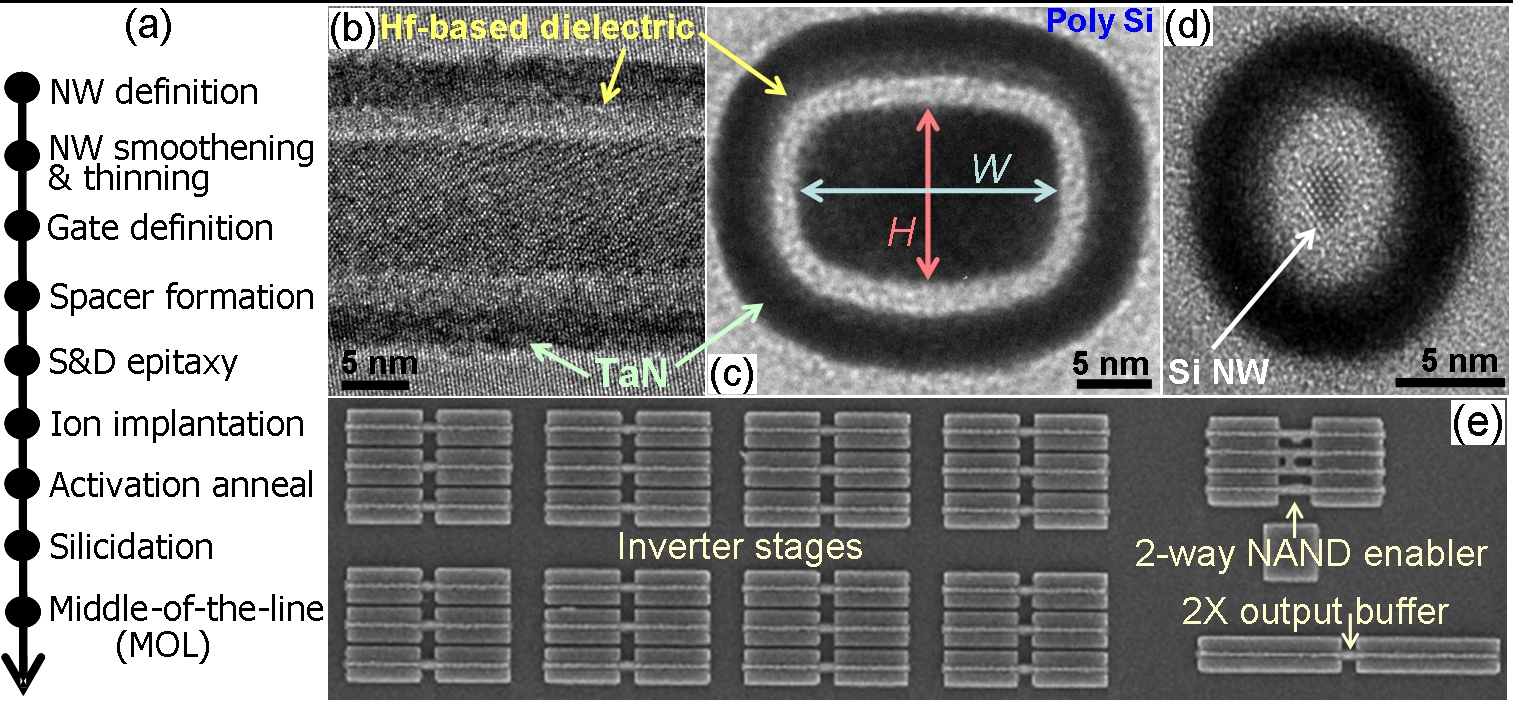
2.3 “Gate-all-around
Silicon Nanowire 25-Stage CMOS Ring Oscillators with
Diameter Down to 3 nm,” Sarunya Bangsaruntip, et al., IBM T. J. Watson Research
Center
High Resolution Images
2.3 Figure 1
2.3 Figure 3
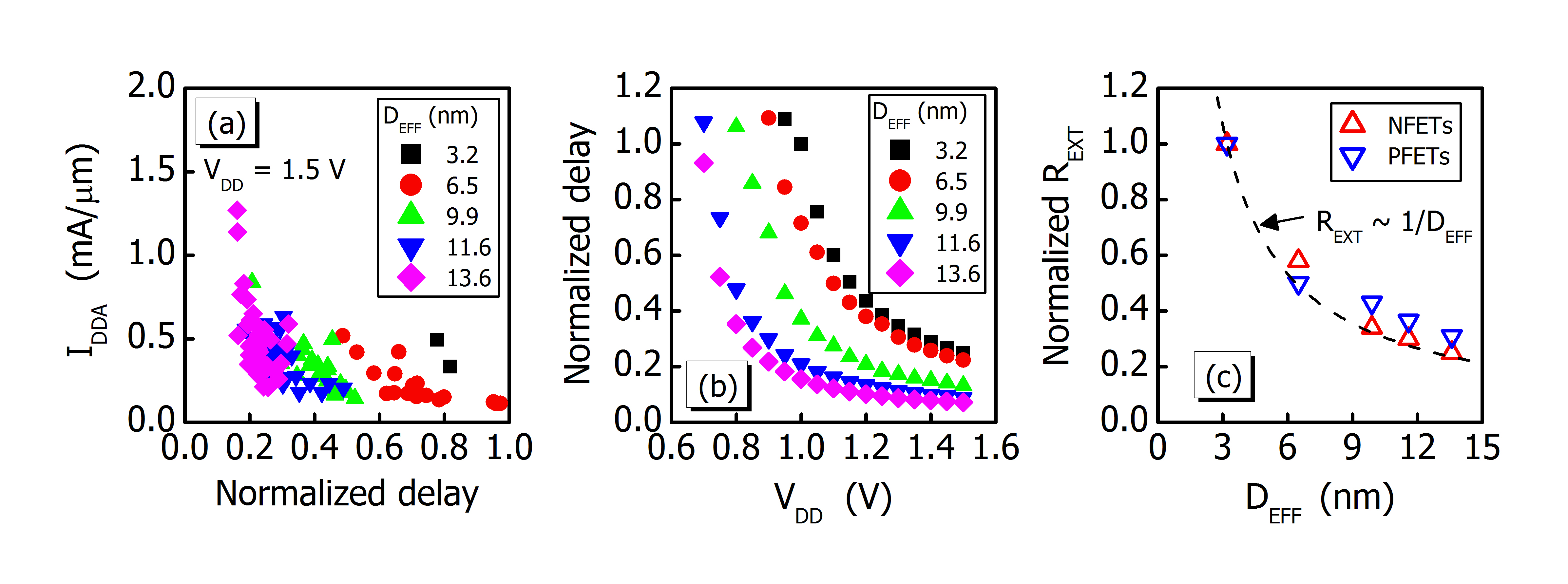
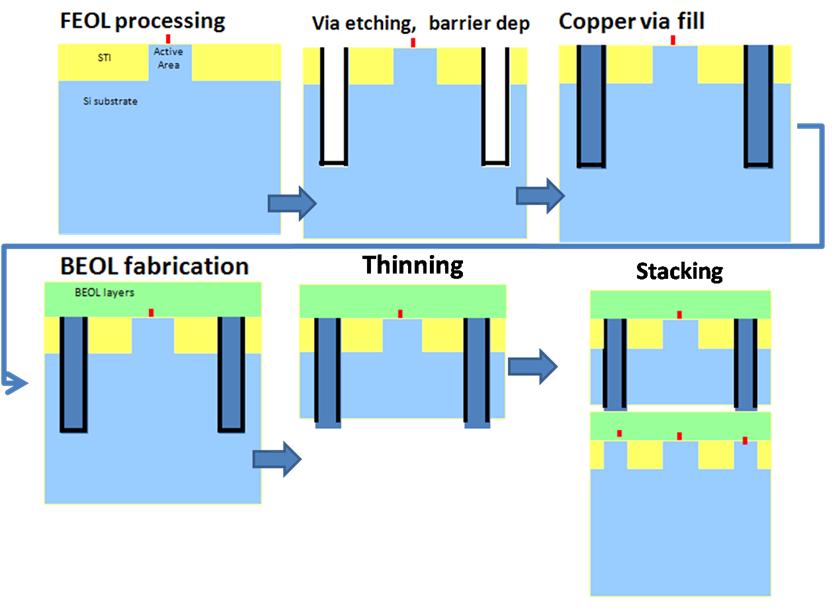
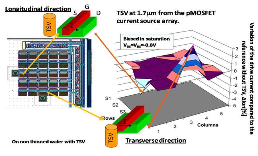
10.3
“Impact of Thinning and Through Silicon Via Proximity on High-k / Metal Gate First CMOS
Performance,” A. Mercha, et al., IMEC, assignee
at IMEC from Panasonic, Qualcom & Samsung
High Resolution Images
10.3 Figure 2
10.3 Figure 3
10.3 Figure 13
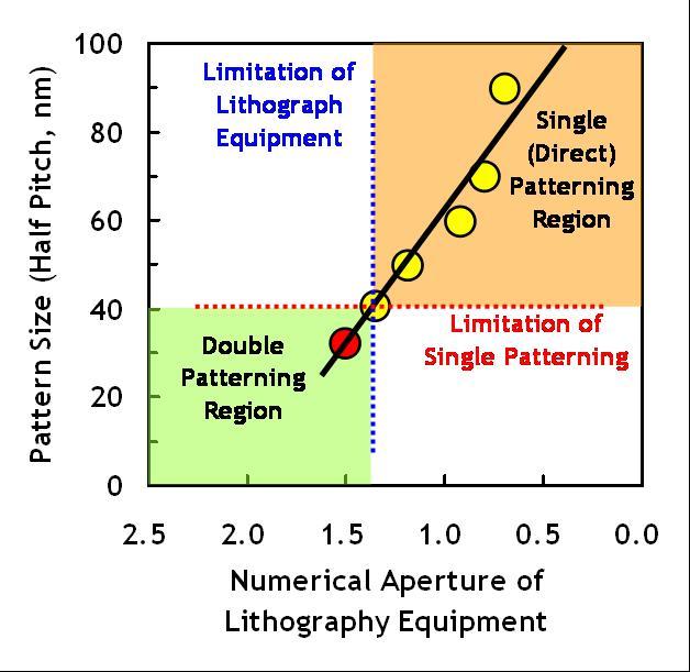
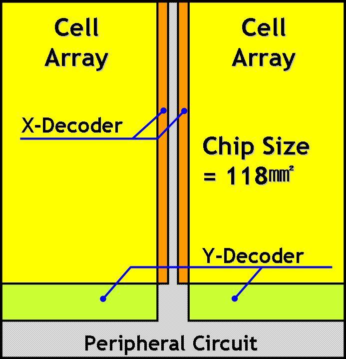
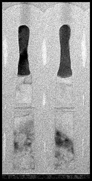
12.1 “32nm
3-Bit 32Gb NAND Flash Memory with DPT (Double
Patterning Technology) Process for Mass Production,” B.T. Park, et al.,
Samsung Electronics, Sungkyunkwan University, South
Korea
High Resolution Images
12.1 Figure 2
12.1 Figure 4
12.1 Figure 5.1
12.1 Figure 5.2
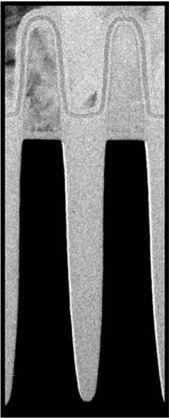
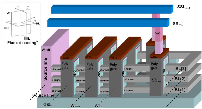
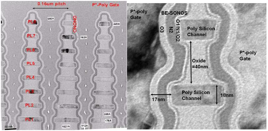
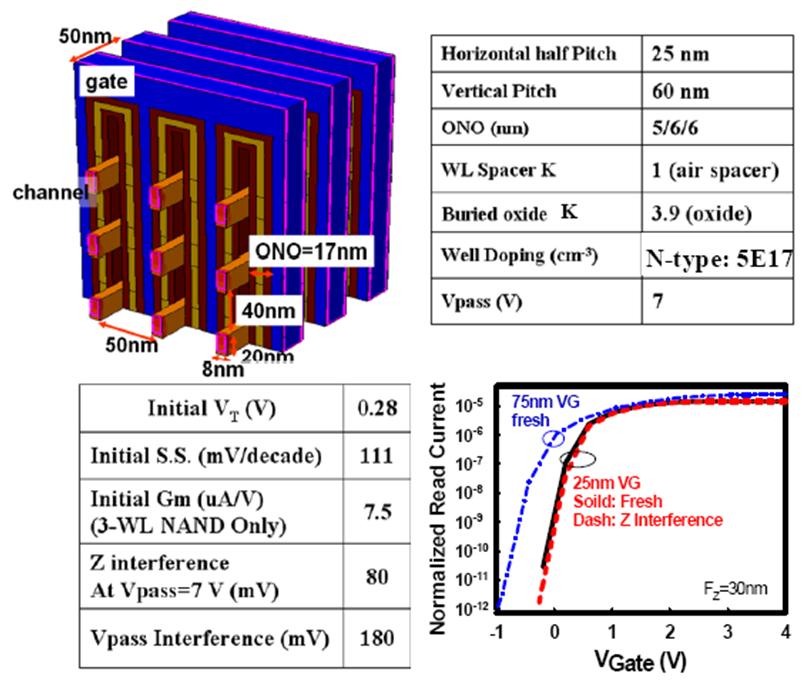
12.4 “A
Highly Scalable 8-Layer 3D Vertical-Gate (VG) TFT NAND Flash Using
Junction-Free Buried Channel BE-SONOS Device,” Hang-Ting Lue, et al.,
Macronix International
High Resolution Images
12.4 Figure 1
12.4 Figure 2
12.4 Figure 11
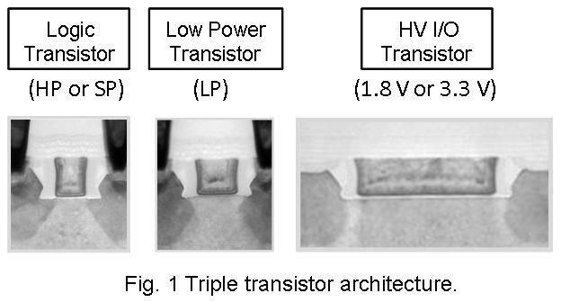
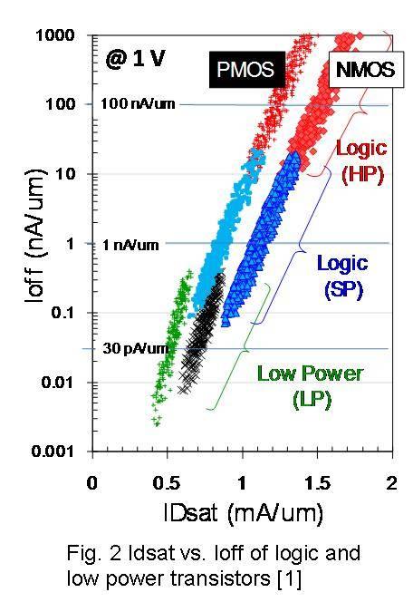
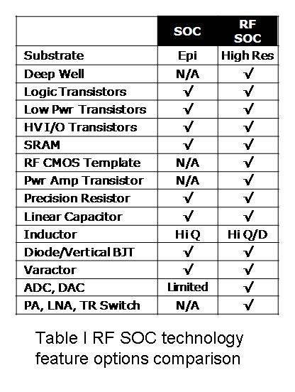
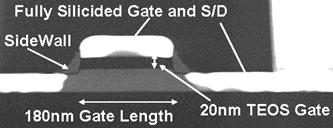
Paper 13.2 “A 32nm Low Power RF CMOS SOC Technology
Featuring High-k/Metal Gate,” Peter VanDerVoorn,
et al., Intel
High Resolution Images
13.2 Figure 1
13.2 Figure 2
13.2 Table I
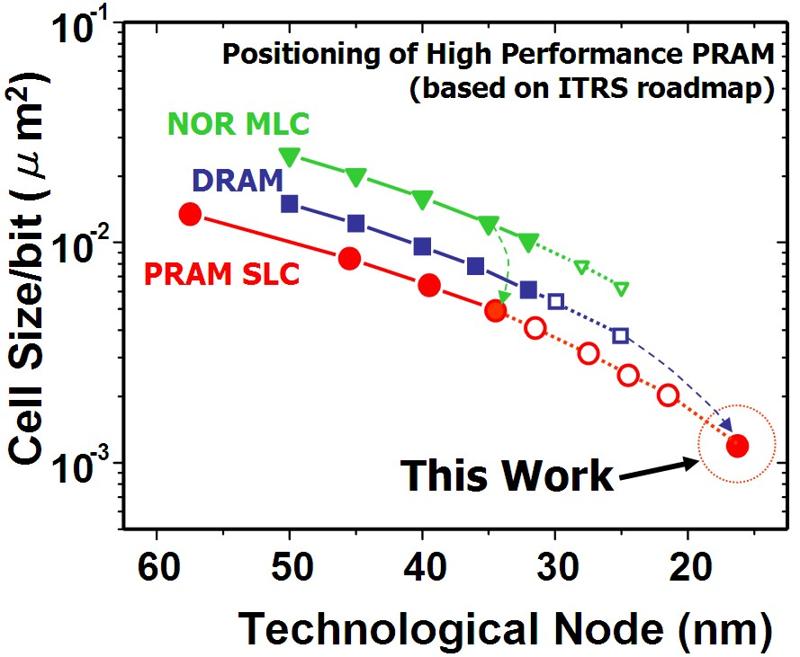
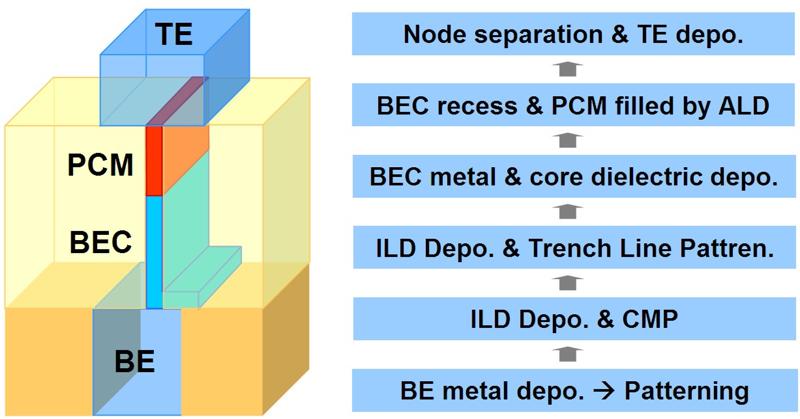
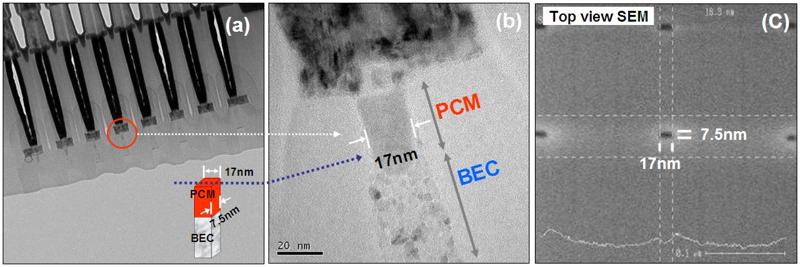
19.3 “High Performance PRAM Cell Scalable to
sub-20nm technology with below 4F2 Cell Size, Extendable to DRAM Applications,”
Ik Soo Kim, et al.,
Samsung Electronics Co., Ltd.
High Resolution Images
19.3 Figure 2
19.3 Figure 3
19.3 Figure 4
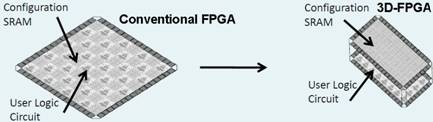
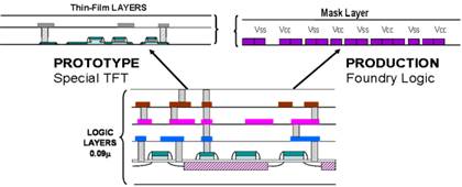
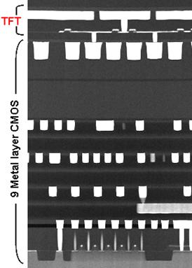
21.1 “World's
first monolithic 3D-FPGA with TFT SRAM over 90nm 9 layer Cu CMOS,”
Tatsuya Naito, et al.,
Toshiba Corp., Covalent Materials Corp., Tier Logic Inc., tei
Technology
High Resolution Images
21.1 Figure 1
21.1 Figure 2
21.1 Figure 4a
21.1 Figure 4b
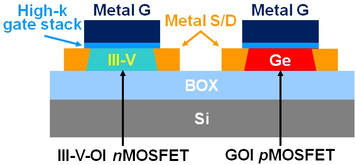
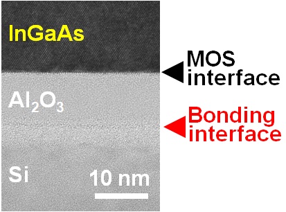
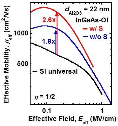
22.3 “High Mobility III-V-On-Insulator MOSFETs on
Si with ALD-Al2O3 BOX layers,” M. Yokoyama, et al., The University of
Tokyo, National Institute of Advanced Industrial Science and Technology &
Sumitomo Chemical Co. Ltd.
High Resolution Images
22.3 Figure 1
22.3 Figure 2
22.3 Figure 8