logo

Plenary, Panel Sessions and Luncheon

The plenary sessions for Technology and also Circuits will each consist of two distinguished industry leaders to describe recent advances and new challenges related to VLSI Technology / VLSI circuits, technology and applications.

The Technology Plenary will be held Tuesday morning, June 14. The Circuits Plenary Session will be held Wednesday morning, June 15.

VLSI Technology and Circuits Symposium evening Panel Sessions are well known for their selection of timely topics and enthusiastic discussions on interesting and provocative topics with technical leaders on the panel to provide all conference attendees an opportunity to participate in the discussions and mix with other attendees and in the audience.

The VLSI Technology Panel Sessions will be held on Tuesday evening, June 14. The Circuits Panel Sessions will be held on Thursday evening, June 16.

Tuesday, June 14

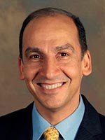
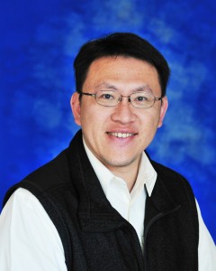
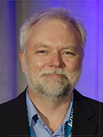
“The Age of Sensors – How MEMS sensors will enable the next wave of new products”, Stephen Lloyd, VP of Engineering and New Product Development, InvenSense, Inc.

This talk will cover the evolution of MEMS sensors from research into the main stream, and how a new generation of sensors will drive several major technology inflections.

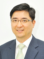
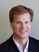
Lloyd

Stephen Lloyd is the Vice President of Engineering and New Product Development for InvenSense. Inc., where he is responsible for Advanced Sensor Technology and all Sensor HW Product Development, a position he has held since December 2008. Steve is focused primarily on highly integrated MEMS motion sensors for consumer applications, such as cell phones, cameras, gaming, wearables, drones, and IOT.  Recent product developments now include automotive and industrial motion sensors, as well as MEMS microphones and other new sensor technologies.

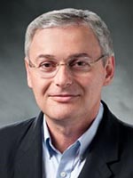
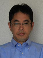
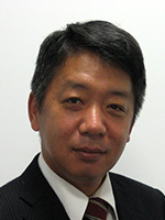
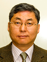
“Intelligent Mobility realized through VLSI”, Takao Asami, Senior Vice President, Nissan

Since the first introduction of a microprocessor into an automobile in 1970’s, the world has been witnessing its dramatic growth as well as its contribution to all aspects of vehicle performance.  At the same time, as the global demand for personal mobility grows continuously, the automotive industry needs to accelerate the development of solutions for the social problems such as environment, energy security, traffic accidents, and urban traffic congestions.  To address these issues, Nissan pursues the ultimate goal, “Zero Emission” and “Zero Fatality”, through the vehicle electrification and the vehicle intelligence.  The electric vehicle is a symbol of electrification that components are fully electrically powered and controlled. Autonomous driving technologies are examples of vehicle intelligence, such as advanced sensing technologies, dynamic driving context interpretation, vehicle maneuver planning and its control.

This session provides an overview of VLSI’s contribution for enhancing vehicle electrification and vehicle intelligence and its perspective of the future mobility system.

AsamiTakao Asami is the Senior Vice President for Research and Advanced Engineering at Nissan, and also the Alliance Global Vice President for the Renault Nissan Alliance. He joined Nissan in 1981 after graduating from the University of Tokyo. He also holds Master of Science in Electrical Engineering from the University of Southern California.  Mr. Asami spent 15 years working through the organization before moving to Nissan Technical Centre North America in Detroit, in the United States, in 1995.  Six years later, as Nissan launched its IT Engineering Department, he returned to Japan to lead the team and drive forward in developing the company’s expertise. In April 2006 he transferred to Nissan’s Alliance partner, Renault. Three years later he was back at Nissan as the Corporate Vice President in charge of the Nissan Research Center.  He was appointed as Senior Vice President in charge of Technology Planning and Advanced Engineering in April 2013 and was appointed to current role in April 2014.

Wednesday, June 15

Enabling Future Progress in Machine-Learning

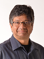
Olivier Temam, Google Inc.

Amazing progress in machine-learning, largely based on deep neural networks, has started to make applications, once considered impossible, such as real-time translation or self-driving cars, a reality. However, even if, on some restricted problems, machine-learning is getting close to human-level performance, we are still far from the capabilities of the human brain. Machine-learning researchers themselves acknowledge that the progress observed in the past 10 years has been largely due to rapid increase in computing performance, allowing to tackle larger neural networks and larger training sets. So the computer systems and circuits communities can play a very significant role in enabling future progress. While GPUs have been a major driver of this recent progress, both the slowing rate of improvement of standard CMOS technology and the need for even faster progress suggest the need to at least explore alternative approaches. In this talk, we will discuss lessons learned from research on architectures for machine-learning, and that some of the hurdles ahead largely lie at the circuit level, but can possibly be overcome in the near future.

temam-olivierAbout Olivier Temam

Olivier Temam received a PhD in computer architecture in 1992, was Assistant Professor at University of Versailles from 1994 to 1999, Professor at University of Paris Sud from 1999 till 2004, then Senior Researcher at Inria from 2004 to 2014 where he led several research groups in computer architecture, before joining Google in 2014. His academic research was focused on hardware neural network accelerators. He gave keynotes at ISCA in 2010 and FCRC in 2015 on hardware neural network accelerators, and he received best paper awards at ASPLOS and MICRO in 2014 for this work.

Accelerating the Sensing World through Imaging Evolution

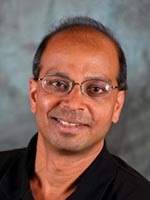
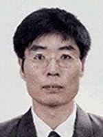
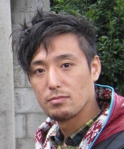
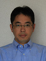
Tetsuo Nomoto, Vice President and Senior General Manager, Sony Semiconductor Solutions Corporation

The evolution of CMOS Image Sensors (CIS) and the future prospect of a “sensing” world utilizing advanced imaging technologies promise to improve our quality of life by sensing anything, anywhere, anytime. Charge Coupled Device image sensors replaced video camera tubes, allowing the introduction of compact video cameras as consumer products. CIS now dominates the market for digital still cameras created by its predecessor and, with the advent of column-parallel ADCs and back-illuminated technologies, outperforms them. CIS’s achieve better signal to noise ratio, lower power consumption, and higher frame rate. Stacked CIS’s continue to enhance functionality and user experience in mobile devices, a market that currently comprises over one billion new image sensors per year. CIS imaging technologies promise to accelerate the progress of sensing world by continuously improving image quality, extending detectable wavelengths, and further improving depth resolution and temporal resolution.

nomoto-tetsuoAbout Tetsuo Nomoto

Tetsuo Nomoto received the B.S. and M.S. degrees in applied physics from Tohoku University, Sendai, Japan, in 1988 and 1990, respectively. In 1990, he joined Olympus Optical Corporation, Nagano, Japan, where he was involved in the development of charge modulation device image sensors. He joined Sony Corporation, Kanagawa, Japan, in 2001, where was engaged in the development of CMOS active pixel sensors. From 2015, he has been responsible for image sensor business for mobile application.

Tuesday, June 14, 8:00 pm – 10:00 pm

“More Moore, More than Moore, or Mo(o)re Slowly”
Moderator: Subu Iyer, University of California Los Angeles

Abstract
Over the past 50 years, rapid advancement of fabrication technology has allowed doubling the number of transistors in VLSI components every two years. This trend has continuously enabled new system features that had been previously impractical if not impossible. As a result of this, the growth of the global semiconductor market has been predominantly fueled by technology scaling in what can sometimes be referred to as a “more of the same is good enough” paradigm. As technology scaling slows down, this dynamic is changing and it is unclear what will drive future growth. Is the industry going to continue a similar path through introduction of new devices and 3D integration? Or is the end of silicon scaling the end of brute force large-scale integration? If that is the case, what is the value of sensor and system integration? Can they generate enough demand to drive growth at a rate comparable to silicon integration? And what is the role of circuit innovation in this environment? One might argue that the “more of the same is good enough” attitude of the past few decades has been a major hindrance for emergence and adoption of many promising ideas at the circuit level? Is the end of scaling a blessing in disguise for the talented circuit designer who would love to tackle a more constrained problem? Renowned experts will attempt to answer these very important questions in this panel.

Circuits Panel

iyer-subramanianSubramanian Iyer teaches at the University of California at Los Angeles. Prior to that he was an IBM Fellow. Over his career, he has worked the area of devices, processes, integration, embedded memory 3D integration, advanced packaging and system integration. His website is chips.ucla.edu. He is an IEEE Fellow and received the IEEE Daniel Noble award in 2012.
de-vivekVivek De is an Intel Fellow and Director of Circuit Technology Research in Intel Labs. He is responsible for providing strategic technical directions for long term research in future circuit technologies and leading energy efficiency research across the hardware stack. He has 240 publications in refereed international conferences and journals and 205 patents, with 30 more patents filed. He received an Intel Achievement Award for his contributions to an integrated voltage regulator technology. He received a PhD in Electrical Engineering from Rensselaer Polytechnic Institute, Troy, New York. He is a Fellow of the IEEE.
lu-nickyAs a researcher, designer/architect, entrepreneur and chief executive, Dr. Nicky Lu has dedicated his career to the worldwide IC design and semiconductor technology over 30 years. He is CEO and Founding Chairman of Etron Technology, Inc. and co-founded several technical companies which are public today. He has MS/Ph.D. degrees from Stanford University, received an IBM Corporate Award and IEEE Solid-State Circuits Technical Field Award. He is an IEEE Fellow and a member of National Academy of Engineering, and serves as Chair of Taiwan Semiconductor Industry Association.
patton-garyDr. Gary Patton is the Chief Technology Officer and Senior Vice President of Worldwide Research and Development at GLOBALFOUNDRIES where he is responsible for GLOBALFOUNDRIES’ semiconductor technology R&D roadmap, operations, and execution. Prior to joining GLOBALFOUNDRIES, Dr. Patton was the Vice President of IBM’s Semiconductor Research and Development Center - a position that he held for eight years where he was responsible for IBM’s semiconductor R&D roadmap, operations, execution, and technology development alliances across multiple locations.  Dr. Patton is a well-recognized industry leader in semiconductor technology R&D with over 30 years of semiconductor experience. Dr. Patton received his B.S. degree in electrical engineering from UCLA and his M.S. and Ph.D. degrees in electrical engineering from Stanford University. He is a Fellow of the IEEE, a member of the IEEE Nishizawa Medal Awards Committee, has co-authored over 70 technical papers and given numerous invited keynote and panel talks at major industry forums.
skotnicki-thomasThomas SKOTNICKI is the STMicroelectronics Company Fellow and Technical Vice-President in charge of Disruptive Technologies at STMicroelectronics Crolles, France. In 2007, he received the title of Professor from the President of Poland, and recently has been appointed the Director of CEZAMAT (Research Consortium) in Warsaw, Poland. The focus of his program at STMicroelectronics is on Low Power / Low Variability for 28nm and beyond CMOS, on innovative device structures, new memory concepts and cells, and on integration of new materials for CMOS. From 2010 he has extended the scope of his program to include Energy Harvesting for autonomous Low Power systems and devices. He holds more than 80 patents on new devices, circuits and technologies. He has presented over 50 Invited Papers and Short Course Lectures, (co-) authored about 350 scientific papers (review based), and several book chapters in the field of CMOS and Energy Harvesting. From 2001 to 2007, he served as Editor for IEEE Transactions On Electron Devices. He has been teaching at EPFL (Lausanne, Switzerland) and SUPELEC (Rennes, France), and has supervised and led to successful defence 26 PhD theses. He has been serving in numerous Conference Program and Executive Committees (IEDM, VLSI, ESSDERC, ECS, SNW, IWJT), Academia Advisory Boards, Governmental Expert Commissions, R&D Program Steering Committees, IEEE Award Committees (JJ Ebers and Frederik Philips), and ITRS (who has been using his/his team software MASTAR for 12 consecutive editions). He is an IEEE Fellow and SEE Senior Member.
vardaman-janE. Jan Vardaman is president and founder of TechSearch International, Inc., which has provided analysis on technology and market trends in semiconductor packaging since 1987. She is co-author of How to Make IC Packages (published in Japanese by Nikkan Kogyo Shinbunsha), a columnist with Printed Circuit Design & Fab/Circuits Assembly Magazine, She is an IEEE CPMT distinguished lecturer and the author of numerous publications on microelectronics market and technology trends. She is a member of IEEE CPMT, IMAPS, MEPTEC, and SEMI. She served two terms on the CPMT Board of Governors. She served on the NSF-sponsored World Technology Evaluation Center study team involved in investigating electronics manufacturing in Asia and on the U.S. mission to study manufacturing in China. Before founding TechSearch International, she served on the corporate staff of Microelectronics and Computer Technology Corporation (MCC), the electronics industry’s first pre-competitive research consortium. She received her B.A. in Economics and Business from Mercer University in Macon, Georgia in 1979 and her M.A. in Economics from the University of Texas at Austin in 1981.
assaderaghi-fariFari Assaderaghi is Senior Vice President and CTO of NXP, Security and Connectivity. He and his team envision system solutions that will dramatically improve the way people live, work, and play. Prior to joining NXP in February 2016, he was Vice President of Advanced Technology at InvenSense. There, he was tasked with expanding the company’s product portfolio beyond inertial sensors to MEMS-based audio solutions, ultrasonic fingerprint sensors, and environmental and health sensors. Fari’s broad interests span semiconductor device physics, process integration, low-power and high performance digital design, mixed signal and RF design, and MEMS. Fari earned his M.S. and Ph.D. degrees in Electrical Engineering from UC Berkeley in 1992 and 1994, respectively. From 1995 to 2001 he was with IBM TJ Watson Research Center where he contributed to the development of the first commercial version of CMOS SOI for VLSI. This technology became the workhorse for IBM’s microprocessors and was used in Apple’s processors, as well as Sony Playstation-3 Cell Processor. Later in his career, he led the adoption of CMOS-based RF solutions for Bluetooth products (at SiliconWave), and high speed data communication circuits and systems, including the breakthrough Terabyte/sec signaling initiative (at Rambus). As Senior VP of Engineering and Operations at SiTime, he led the first development and broad commercialization of MEMS-based timing products, as alternatives to legacy crystal oscillators. During his tenure, company’s shipments grew to over 50 million units/year. Dr. Assaderaghi’s quest has been identifying nascent technologies and paving their way into broad adoption. He has given many invited talks, contributed to more than 100 technical papers, and has attained 57 patents.

Tuesday, June 14
8:00 p.m. – 10:00 p.m.

“How Moore’s Law, Industry Consolidation, and System Trends are Shaping the Memory Roadmap”
Moderators:  Gary Bronner, Rambus and Fred Chen, Winbond

Preliminary questions for the panel:

  • Moore’s Law – are we at the end for the scaling of memories?  What’s the metric of interest?  Capacity? Design Rule? Cost? Performance? Power/Energy Efficiency?
  • Why do we need anything beyond DRAM and Flash? What is the impact of slowing DRAM cost reduction on their use in products and systems?
  • For Flash Technology
  • Will conventional 2D NAND survive or 3D NAND completely replace it?
  • What are the technical limits for 3D NAND?  When does it stop scaling?
  • For DRAM Technology
  • Will the introduction of compact, high BW memory (HBM) lead to a change in memory hierarchy)?
  • Where and when will 3D stacked memory become a volume product?
  • Where and when will new/emerging memory technology first enter the market? What is the customer adoption status?
  • How would the memory hierarchy change with the introduction of SCM (storage class memory)?
  • Industry consolidation – how many vendors does the world need?

Abstract:

The roadmap for memory, both DRAM and Flash, has historically been driven by a self-fulfilling prophecy – memory cost must drop 35% / year on a cost per bit basis.  Moore’s law drove this exponential decrease in cost and increase in memory density for over 3 decades.  But the last decade has seen interesting modifications to this historical trend.  The emergence of NAND Flash memory led to even faster drops in price, with NAND now 16x cheaper than DRAM on a cost/bit basis.  DRAM scaling limits are causing DRAM density improvement to slow and the price gap to widen.   NAND Flash continues on a classical price/density roadmap but its performance is not sufficient to replace DRAM.   Current systems and applications are facing a “Memory Wall” – cheap Flash bits don’t meet CPU performance needs while DRAM bits are no longer cheap enough to meet the capacity needs of multicore CPUs.  This has triggered a burst of innovation at all levels – technology, system, and software, creating a myriad of possibilities to be considered.

This panel will debate the technology roadmaps for DRAM, FLASH, SCM (storage class memory) and eNVM (embedded Non Volatile Memory) in light of the fundamental problems around memory cost, performance, and power.   Can any of the emerging NVM technologies provide compelling solutions to current computer system and application needs?  Which industry will drive the new memory technology – data centers or mobile chip vendors?  What memory (or combination of memories) gives the lowest total cost of ownership?  How will computer systems handle new levels of memory hierarchy?  How does industry consolidation and the emergence of new players in the memory industry affect the roadmap? These and other questions raised from the audience will be addressed by a distinguished panel of experts from industry.   It is a most interesting time to be involved in the memory world!

Memory Panel

bronner-garyGary Bronner is Vice President of Rambus Labs, where he is responsible for his company’s long term research in memory devices and systems.  Prior to joining Rambus in 2006, he was at IBM where he was responsible for the development of many generations of DRAM technology.  He is author or co-author of over 80 issued US Patents along with numerous journal and conference publications.  He received his ScB degree from Brown University and MS and PhD degrees from Stanford University.  He is a Fellow of the IEEE.
chen-frederickDr. Frederick Chen received his Ph.D. in Applied Physics from Cornell University, after demonstrating the first artificial dielectric diffractive optical element at a visible wavelength. After receiving his Ph.D., he worked at Intel's Mask Operations, developing advanced photomasks for the 0.25 um to 45 nm nodes as well as for EUV and double patterning. In 2005, he moved to Taiwan's Industrial Technology Research Institute, where he worked on developing and modeling advanced phase change memory structures and later HfO2-based resistive memory. At ITRI, he and his patterning team also developed self-trimming double patterning, which was implemented in the cross-spacer phase change memory published at IEDM 2007. He is currently at Winbond Electronics, where he is helping to improve RRAM reliability and establishing the filamentary RRAM model.   
borkar-shekharShekhar Borkar is an Intel Fellow, an IEEE Fellow, and Director of Extreme-scale technologies at Intel Corporation. He served as the TPC chairman of VLSI Circuit Symposium in 2002, and as the conference chairman in 2004. Shekhar was an adjunct faculty at Oregon Graduate Institute, taught graduate course on VLSI design for more than 10 years. His research interests are low power, high performance digital circuits, high speed signaling, and system level optimization. Shekhar holds M.Sc. in Physics from University of Bombay in 1979, and MSEE from University of Notre Dame in 1981.
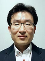
kono-takashiTakashi Kono received the B.S. and M.S degrees in electronic engineering from University of Tokyo, Tokyo, Japan, in 1992 and 1994, respectively. In 1994, he joined Mitsubishi Electric Corporation. From 1994 to 2002, he was engaged in the research and design of DRAMs from 64Mb to 512Mb including synchronous DRAMs and DDR/DDR2 DRAMs. After transferring to Renesas Technology Corporation in 2003, he worked on the development of low-power pseudo-SRAM and high-density flash memories. He is currently with Renesas Electronics Corporation, where he has been supervising the development of advanced embedded Flash memory for high performance Flash MCUs. Since 2014, he has been serving for memory sub-committee of ISSCC.
lee-jaejinJaejin Lee received the B.A degree at Physics from Seoul National University in Seoul, Korea in 1986. He has been working as DRAM design engineer for over 25 years at SK Hynix and he was always on the edge of the first developments of all the types of DRAMs. In recent years he completed the development of HBM1 on general responsibility and now he is leading Design Innovation Lab to envision and realize the concepts of future memories as a Research Fellow at SK Hynix. He has over 50 US patents.
lim-junheeJunhee LIM worked at Samsung for the past 15 years, participating the DRAM research and developing program from 5x nm to 2x nm technology node and late managing the design and fabrication of the peripheral transistor of DRAM. Since 2015, he has been involved in developing Vertical NAND Flash device at the R&D center in Samsung Electronics. He earned his B.S. in electrical engineering from the Seoul National University, Korea.
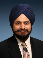
sandhu-gurtejGurtej S. Sandhu is Senior Fellow and Director of Advanced Technology developments at Micron Technology, Inc. In his current role, he manages the Advanced Memory Technologies Roadmap and forward looking Research & Development at Micron. He received degree in electrical engineering at the Indian Institute of Technology, New Delhi and a Ph.D. degree in physics at the University of North Carolina, Chapel Hill, in 1990. Dr. Sandhu then joined Micron Technology, where he has been in a number of engineering and management roles responsible for process technology development, pilot manufacturing and transfers to manufacturing. He has been associated with microelectronics technology for over 20 years and has pioneered several process technologies which are currently employed in mainstream semiconductor chip manufacturing. Moreover, he was involved with introduction of a number of Atomic Layer Deposition (ALD) based processes and innovative patterning techniques for memory chip technology. Dr. Sandhu has authored over 35 technical papers and several hundred issued U.S. patents. Dr. Sandhu is Fellow of IEEE.
sprinkle-robRob Sprinkle is a Technical Lead in Google's Data Center Infrastructure Advanced Technology Team. He is responsible for working with established and emerging memory technology companies to track and influence strategic technical directions, and internally to determine best uses of custom and emerging memory technologies and designs in the data center infrastructure. Previously he was the Technical Lead for the concept and hardware design of Google's first custom NAND Flash storage tier, and is a recipient of Google's second highest corporate recognition award. Prior to 2006, he was a PCB and ASIC/FPGA designer/manager at Teradyne. He received a BSEE from the Virginia Military Institute and has been issued numerous patents with others pending.

Thursday, June 16
8:00 p.m. – 10:00 p.m.

“Top Circuit Techniques: Life With and Without Them”
Organizer: Dejan Markovic, University of California, Los Angeles and Kenichi Okada, Tokyo Institute of Technology
Moderator:   Un-Ku Moon, Oregon State University

Panel consisting of experts from different areas will provide a review of the highest-impact circuit techniques, and give examples of how these techniques brought significant system advances. After the opening statement from each of panelists, limited to one technique, audience can debate to gauge the impact of those techniques. At the end of the panel discussion, everyone can join to vote the top three circuit techniques in 2016.

Top Circuit Techniques

unkoo-moon-photoUn-Ku Moon received the B.S. degree from the University of Washington, the M.Eng. degree from Cornell University, and the Ph.D. degree from the University of Illinois at Urbana-Champaign. He has been with the Oregon State University since 1998. He was with Bell Labs from 1988 to 1989, and from 1994 to 1998. His technical contributions have been in the area of analog and mixed-signal integrated circuits including analog filters, timing recovery, PLLs, data converters, and low voltage circuits.
Miki-photoTakahiro Miki received B.S., M.S., and Ph.D. degrees in electronics engineering from Osaka University, Japan, in 1980, 1982, and 1994. He joined the LSI Research and Development Laboratory, Mitsubishi Electric Corporation, Tokyo, Japan, in 1982 and moved to the Advanced Analog Technology Division, Renesas Technology Corporation, Japan, in 2003. He is currently with 1st Solution Business Unit, Renesas Electronics Corporation. In these companies, he has been engaged in the research and development of analog and mixed-signal circuits, including data converters, wireless communication circuits. Dr. Miki is a member of the Institute of Electronics, Information and Engineering (IEICE) of Japan and a senior member of IEEE.
meng-fan changDr. Chang is a full Professor at the Dept. of Electrical Engineering of National Tsing Hua University (NTHU), Taiwan. He also serves as the Associate Executive Director of Taiwan’s National Program for Intelligent Electronics (NPIE) since 2011. Before his joint NTHU in 2006, he had worked in industry over 10 years. During 1997~2006, he had developed SRAM/ROM/Flash macros/compilers in Mentor Graphics (New Jersey, US), TSMC (Taiwan), and Intellectual property Library Company (Taiwan). His research interests include circuit designs for volatile and nonvolatile memory, 3D-Memory, spintronics and memristor logics, computing-in-memory, and circuit-device-interaction for non-CMOS devices. Since 2010, Dr. Chang has authored or co-authored more than 40 conference papers (including 11 ISSCC, 11 VLSI Symposia, 5 IEDM, and 4 DAC papers), as well as 25+ IEEE journal papers. He also hold more than 30 U.S. patents. He has been serving on technical program committee for ISSCC, IEDM, A-SSCC, ISCAS, and numerous international conferences. He also is serving as the associate editor for IEEE TVLSI, IEEE TCAD and IEICE Electronics. He received the Academia Sinica Junior Research Investigators Award in 2012, the Ta-You Wu Memorial Award of National Science Council (NSC-Taiwan) in 2011. He has also received numerous awards from the Taiwan National Chip Implementation Center (CIC), Macronix Golden Silicon Awards, ITRI and NTHU.
abidi-headshotAsad Abidi received the BSc (Hons) from Imperial College, London, and the MS and PhD degrees from the University of California, Berkeley, all in Electrical Engineering. After working at Bell Laboratories, Murray Hill, NJ, in 1985 he joined the faculty of the University of California, Los Angeles, where he is Distinguished Chancellor’s Professor of Electrical Engineering.
ippei-akita-photoIppei Akita received the Ph.D. degrees in Electronic and Information Engineering from Toyohashi University of Technology. In 2008, he joined Toshiba Corporation where he engaged to develop AD/DA converters and opt-electronic integrated circuits (OEICs) for wireless/wireline communication systems. Since 2011 he has been with Toyohashi University of Technology as an Assistant Professor. His current research interests include the design of analog mixed-signal LSIs and the development of packaging technique using flexible thin-film devices for implantable brain-machine interfaces and ultra-low-power physical sensor devices.
khellah-photoMuhammad M. Khellah is a principal research scientist at Intel Labs, where he leads research on low-power circuits and architectures with particular focus on power management, resiliency, and embedded memory. After obtaining his PhD from the University of Waterloo Canada in 1999, he joined Intel and was first involved in the design of SRAM caches for the Pentium microprocessor products. He has published over 70 technical papers in refereed international conferences and journals, and has 74 patents granted, and a few pending – all in the area of VLSI design. Dr. Khellah served as an associate editor for the IEEE TCAS-I, and as technical program co-chair for the 2014 IEE/ACM ISLPED. He currently serves as the 2016 ISLPED general co-chair, and as a TPC member of the IEEE CICC.
adrian tangAdrian Tang, from NASA's Jet Propulsion Laboratory and the University of California, Los Angeles, develops CMOS-based space instrumentation for future NASA planetary missions exploring the outer planets (Jupiter, Saturn) and their moons, as well instruments for climate and atmospheric science here on Earth. His primary research focus is SoC development for spectroscopic, radiometric, and radar instrument systems.
aberg-photoAndreas Burg received his Dipl.-Ing. degree from the ETH Zurich in 2000 and the Dr. sc. techn. degree also from ETH in 2006. In 1998, he worked at Siemens Semiconductors, San Jose, CA and during his doctoral studies, at the Bell Labs Wireless Research Labs for a total of one year. In 2007 he co-founded Celestrius, where he worked as Director for VLSI. In January 2009, he joined ETH Zurich as SNF Assistant Professor and since January 2011, he has been a Tenure Track Assistant Professor at the Ecole Polytechnique Federale de Lausanne (EPFL). He has served on the TPC of various conferences on VLSI, signal processing, and communications. He was a TPC co-chair for VLSI-SoC 2012 and is a TCP co-chair of ESSCIRC 2016 and SiPS 2017. He served as an Editor for the IEEE Transaction of Circuits and Systems in 2013 and is on the Editorial board of the Springer Microelectronics Journal and the MDPI Journal on Low Power Electronics and its Applications.

It’s All a Common Platform – How Do I Build a Differentiated Product?”
Organizers: Fatih Hamzaoglu Intel and Masanori Hashimoto, Osaka University
Moderator:  Ajith Amerasekera, Texas Instruments

Chip industry has been very competitive in recent years as semiconductor Foundry, Memory suppliers, IP developers, and EDA tools have diminished to few players. With very tight TTM (Time to Market) and cost requirements, vendors have limited value options to add to their products to differentiate from competition. The panelists will discuss how innovation, software hardware co-design, cost vs. performance optimization, user interface and other factors can differentiate their products even with common infrastructure.

It’s All a Common Platform

Ajith AmerasekeraDr. Ajith Amerasekera is a TI Fellow and IEEE Fellow, and CTO for TI’s High Performance Analog business with responsibilities in strategic technology, new business development and engineering execution. He has made technical contributions over a wide range of areas in over 25 years in the semiconductor industry, from working on the first submicron transistor development to design of high performance analog circuits and systems.  His innovations, including performance analog circuits, high voltage and high current design, and new transistors, have been in use for two decades and are in many of TI’s leadership products.  After receiving his Ph.D. in semiconductor physics from Loughborough University, England, in 1986, he worked at Philips Research Labs, Eindhoven, The Netherlands, on the first submicron semiconductor development. In 1991, he joined Texas Instruments in Dallas working in the VLSI Design Labs before moving to technical leadership roles in TI’s business divisions.  He has 30 issued patents, and has published over 150 papers in technical journals and conferences, as well as 4 books on Integrated Circuits. Ajith has served on the technical program committees of a number of international conferences including the VLSI Symposium on Circuits, the ISSCC, and the IEDM.  In 2016, he was named as Executive Director of the Berkeley Wireless Research Center at UC Berkeley.
Steve YoungSteve Young is a Xilinx Fellow with 32 years in the industry and 23 years at Xilinx. Prior to Xilinx he worked at Hewlett Packard and a startup company. At Xilinx, he led architecture definition for the first several generations of Virtex FPGA products. He now focuses on future silicon technology and how Xilinx architecture can adapt to changing capabilities. He has worked on FPGA interconnect, die stacking, circuit design, layout, and metal planning. He has roughly 200 issued patents.
rob_aitkenRob Aitken is a Fellow and Director of Technology at ARM Research, San Jose California. He has been with ARM since 2004, and was previously with Artisan Components, Agilent Technologies, and Hewlett-Packard. His areas of responsibility at ARM include low power design, library architecture for advanced process nodes, and design for manufacturability. He has published over 70 technical papers in refereed journals and conferences, on topics ranging from the statistics of memory bit cell variability to testing techniques. He holds 20+ patents and is an IEEE Fellow.
Hugh_MairHugh Mair is Senior Director of Advanced CPU and Technology at Mediatek in Austin where he has worked since 2012. He graduated from the University of Glasgow in 1990, and joined the mixed-signal design group of Texas Instruments in Dallas. His work at TI focused on high-speed, low-power mixed signal and digital circuit design, including high-rate/long-reach SERDES, low-power SRAM, and power management for advanced CMOS. At Mediatek his organization is responsible for achieving best-in-class PPA of Smartphone CPUs. Hugh has helped author 16 papers, and invent over 45 patents.
SukLeeMr. Suk Lee has over 25 years of experience in the Semiconductor, EDA, and IP industries and is currently Senior Director of Design Infrastructure Marketing Division at TSMC. He has held engineering, marketing, and senior management positions at LSI Logic, Texas Instruments, Cadence, and Magma Design Systems where he was GM and VP of the Custom Design Business Unit. He holds a Bachelor of Engineering from MIT and Master of Science from the University of Toronto. At TSMC Mr. Lee is responsible for the EDA, IP, and Design Services Alliances which are components of the Open Innovation Platform.
Hoi-Jun YooProf. Hoi-Jun Yoo is the full professor of Department of Electrical Engineering at KAIST and the director of SDIA(System Design Innovation and Application Research Center). From 2003 to 2005, he was the full time Advisor to the Minister of Korean Ministry of Information and Communication for SoC and Next Generation Computing. His current research interests are Bio Inspired Intelligent SoC Design, Wearable Computing and Wearable Healthcare. He published more than 200 papers, and wrote 5 books including "Biomedical CMOS ICs"(2011, Springer). Dr. Yoo received the National Medal for his contribution to Korean Memory Industry in December of 2011, the Korean Scientist of the Month award in Dec. 2010, Best Research of KAIST Award in 2007, Design Award of 2001 ASP-DAC, and Outstanding Design Awards 2005, 2006, 2007, 2010, 2011, 2014 A-SSCCs, and Best Demo Award of ISSCC 2016. He is an IEEE Fellow, a member of the executive committee of Symposium on VLSI, and A-SSCC. He was the TPC Co-Chair of ISWC 2010, IEEE Distinguished Lecturer('10-'11), and Asia Chair of ISSCC(‘10-‘11). He was TPC Chair of ISSCC 2015, Vice Chair of ISSCC 2014, Technology Direction Sub-Committee Chair of ISSCC 2013, a member of Executive Committee of ISSCC 2008-2015 and recognized as the top 4 paper-contributor for 2004-2013 ISSCCs and top 10 paper contributor for 1954-2013 ISSCCs.
takashi_konoTakashi Kono received the B.S. and M.S degrees in electronic engineering from University of Tokyo, Tokyo, Japan, in 1992 and 1994, respectively. In 1994, he joined Mitsubishi Electric Corporation. From 1994 to 2002, he was engaged in the research and design of DRAMs from 64Mb to 512Mb including synchronous DRAMs and DDR/DDR2 DRAMs. After transferring to Renesas Technology Corporation in 2003, he worked on the development of low-power pseudo-SRAM and high-density flash memories. He is currently with Renesas Electronics Corporation, where he has been supervising the development of advanced embedded Flash memory for high performance Flash MCUs. Since 2015, he has been serving for memory sub-committee of ISSCC.
mark-doranMark Doran is an Intel Fellow and the chief platform software architect within the System Software Division for the Software and Services Group at Intel Corporation. As lead architect for the Unified Extensible Firmware Interface (UEFI) program and the company’s implementation of UEFI, codenamed “Tiano,” he develops industry standards-based firmware for Intel architecture systems. Doran also serves as president of the UEFI Forum, a non-profit trade organization that develops the primary de jure industry standards for platform firmware. Before assuming his current position at Intel, Doran was the program manager for the Intel boot initiative. That initiative, which involved defining a boot solution for Intel Itanium processor-based platforms, led to the Extensible Firmware Interface (EFI). Earlier in his Intel career, Doran served as manager of the Applications Solution Center, and as the developer and author of the Multiprocessor Specification (MPS), the first recipe for commodity multi-CPU, PC-compatible computers and operating systems. He joined Intel in 1994 as a software engineer for UNIX operating system development. Before coming to Intel, he was with UNIX International and served as a consultant in open systems development for The Instruction Set Ltd. in London. Doran is the author of two books and numerous articles published in technical journals. He holds 19 patents in the field of platform firmware and system boot architecture, with another four patents pending, and he is a four-time winner of the Intel Achievement Award for technological innovation and his contributions to firmware engineering. Doran earned a bachelor’s degree in computer science with electronic engineering from University College, London University, in the United Kingdom.

As semiconductor industry approaches seemingly finite limits of physical scaling, a number of inflections are unfolding around us that may require us to rethink how we design, develop and manufacture semiconductor devices. Sensing, positioning, energy-aware and predictive systems are becoming the norm, opening up wider applications and enormous growth potential for semiconductor industry. Yet, implementation of such technologies from research to reality also poses technical and business challenges. Such systems require ultra-low power, always-on sensing, connectivity, vast embedded and discrete memory, smart energy sources and management – all wrapped in to ever smaller form factors. IoT, self-driving automobiles, next generation 5G networks, machine learning, brain-inspired computing, virtual/immersive reality and many other emerging trends will also need large investments for successful deployment and business models for ROI. The cost of developing such technologies, acceptable standards, security protocols, inter-platform operability, etc., will need unprecedented collaboration in the industry. The panel will deliberate on these topics and discuss trends, applications that are shaping around us, industry needs, infrastructural/manufacturing gaps and economic challenges.

Executive Panel

patton-garyDr. Gary Patton is the Chief Technology Officer and Senior Vice President of Worldwide Research and Development at GLOBALFOUNDRIES where he is responsible for GLOBALFOUNDRIES’ semiconductor technology R&D roadmap, operations, and execution. Prior to joining GLOBALFOUNDRIES, Dr. Patton was the Vice President of IBM’s Semiconductor Research and Development Center - a position that he held for eight years where he was responsible for IBM’s semiconductor R&D roadmap, operations, execution, and technology development alliances across multiple locations.  Dr. Patton is a well-recognized industry leader in semiconductor technology R&D with over 30 years of semiconductor experience. Dr. Patton received his B.S. degree in electrical engineering from UCLA and his M.S. and Ph.D. degrees in electrical engineering from Stanford University. He is a Fellow of the IEEE, a member of the IEEE Nishizawa Medal Awards Committee, has co-authored over 70 technical papers and given numerous invited keynote and panel talks at major industry forums.
TC Chen (1)Dr. Chen is currently an IBM Fellow and V.P. at the IBM Thomas J. Watson Research Center, where he serves as the adviser to IBM Research Director in the strategic areas of physical science including nano-science & technology, advanced semiconductor science and technology, subsystem integration, and advanced communication technology. For 30 years, Dr. T.C. Chen has driven major innovations in silicon microelectronics technology with contributions spanning across research, development and product manufacturing. His technical and managerial leadership in understanding and developing advanced bipolar, complimentary metal-oxide semiconductor (CMOS) and dynamic random access memory (DRAM) technology has played a critical role in placing IBM as the leader of semiconductor technology. Technology developed under Dr. Chen’s guidance has impacted mainframe computing systems used worldwide for scientific, banking, and other business applications and has advanced the global semiconductor industry as a whole. During the 1980s, Dr. Chen conducted pioneering work on the polysilicon emitter/single crystal silicon interface that led to the world’s first double-poly bipolar technology to manufacturing. The successful commercialization of this technology formed the basis of semiconductor devices that were deployed in the IBM S/390 mainframe computers. Beginning in 1999, Dr. Chen helped lead an IBM team that demonstrated the first commercial microprocessor using silicon-on-insulator technology for high-performance logic. He also personally led IBM’s high-k/metal-gate CMOS development, which was one of the biggest changes to silicon microelectronics technology in decades. Dr. Chen is a strong advocate of international collaboration in technology development. During the 1990s, he led a multinational alliance for advancing trench-capacitor DRAM technology, and his technical contributions led to the announcement of the world’s fastest and smallest 256-Mb DRAM in 1995. His successful multinational development programs became the models for subsequent IBM joint-development projects with semiconductor companies worldwide. An IEEE Fellow, Dr. Chen is also a Fellow of the American Physical Society and of the School of Engineering, University of Tokyo. In 1999 he was named IBM Fellow for sustained technical excellence and leadership. Dr. Chen was honored with the IEEE Ernst Weber Engineering Leadership Recognition in 2011. Other honors include being named the 2005 Asian-American of the Year and receiving the 2006 Yale Science and Engineering Association Award for Distinguished Service to Industry, Commerce or Education. Dr. Chen received his bachelor’s and master’s degrees in physics from National Cheng-Kung University, and master’s and doctorate degrees in Engineering and Applied Science from Yale University.
sung joo hongDr. Sung-joo Hong is executive vice president of R&D at SK hynix. He leads the organization responsible for various research and development activities that extend from DRAM, NAND to New Memory. He first joined Hyundai Electronics Industries Co., Ltd (Currently SK hynix) as a device engineer for DRAM process integration in 1986. Later, he was responsible for Device at Memory Research Center. He was appointed as the head of DRAM Product Development, and then promoted to executive vice president of R&D in December 2014. Dr. Hong gained an outstanding recognition for his role in successful development of the world’s first ultra-high density 128GB DDR4 DRAM module for Server application in 2014; the world’s first HBM incorporating TSV technology in 2014; the world’s smallest 2ynm 4G DDR3 DRAM in 2013; the world’s smallest 2x/2ynm 64Gb MLC NAND Flash Memory in 2012; and the world’s first 20nm High Speed Low Power premium 2Gb/4Gb DDR3 DRAM in 2012. Dr. Hong received B.A in physics from Seoul National University, M.S. and Ph.D. in physics from Korea Advanced Institute of Science and Technology (KAIST). He became a member of The National Academy of Engineering of Korea in 2016. He won the Presidential Prize at Korea Semiconductor Technology Award in 2006 and received the 2nd highest medal (Hyeoksin Medal) in the 5 level of the Order of Science and Technology Merit in 2015. Throughout his career in the semiconductor industry, he presented more than 56 papers at numerous international semiconductor conferences.
steve lloydStephen Lloyd is the Vice President of Engineering and New Product Development for InvenSense. Inc., where he is responsible for Advanced Sensor Technology and all Sensor HW Product Development, a position he has held since December 2008. Steve is focused primarily on highly integrated MEMS motion sensors for consumer applications, such as cell phones, cameras, gaming, wearables, drones, and IOT. Recent product developments now include automotive and industrial motion sensors, as well as MEMS microphones and other new sensor technologies. Prior to InvenSense, Steve worked at several semiconductor companies, including service from 2004 to 2008 at Beceem Communications, as Executive Vice President of Engineering, where he helped developed one of the first production WiMAX modem chipsets. From 2002 to 2004, he served as Executive Director of RF IC Design for Skyworks Solutions, and from 1997 to 2002, he served as an Executive Director of Conexant Systems, where he was responsible for developing highly integrated radio IC’s for Cordless, CDMA, and GSM standards. Mr. Lloyd received his B.S. in Electrical Engineering from the University of California, Berkeley. Steve was awarded the 2015 MEMS Engineer of the Year by the MEMS Industry Group. He has served as both technical program chair and general chair for the IEEE RFIC Symposium, and has authored over 10 patents and various technical papers.
Marie-N. SemeriaMarie-Noëlle Semeria became CEO of CEA-Leti in October 2014, succeeding Laurent Malier. She was also named president of the Carnot Institutes Network, an association of more than 30 French research centers and laboratories. During her previous 18 years at CEA, she held various senior-management and strategydevelopment positions, and helped secure numerous patents. She served as Leti’s deputy director from 2007-2011. Most recently, she was chief scientist at CEA Tech, the CEA research unit that includes Leti, Liten and List. In that position, she was in charge of developing and implementing the unit’s scientific and technological goals, coordinating with industrial partners and establishing strategic partnerships with academic labs. As Leti’s Chief Executive Officer, she directs the activities of one of Europe’s largest microand nanotechnologies research institutes, which employs more than 1,700 people and has a portfolio of more than 2,200 patents. She joined Leti in 1996 as project manager, and also served as head of the institute’s Thermal Treatment Lab from 1996-1999. From 2003-2007, she was the microelectronics program manager. While serving as deputy director, she took on the additional responsibility of defining the institute’s strategy, working closely with the Carnot Institutes Network. She began her career at Sagem, the high-tech unit of the SAFRAN Group. At Sagem, she served as project engineer and was promoted to manufacturing chief engineer, focusing on magnetic memory technologies. Semeria left Sagem after seven years to join the French start-up PixTech as chief architect, working on emissive flat-screen technology. After three years at PixTech, she joined Leti in 1996. In 2011, she was awarded the Legion of Honor, and in 2015 the French Order of Merit, France’s highest professional accolades. Marie-Noëlle Semeria is a member of the French and European Physics Societies. She has also served as a member of the National Committee of the French National Center for Scientific Research (CNRS) and the Superior Council of Research and Technology. She is currently a member of the Executive Committees of ANR (the French National Research Agency) and CNRS, and the Coordinating Committee of the Allistene alliance, the science and digital technology alliance. She received a doctorate of science in solid-state physics from Joseph Fourier University in Grenoble.

MaharbizHighRes1


“Cyborg Insects & Other Things; Building Interfaces Between the Synthetic & the Multicellular”
Speaker:  Michel Maharbiz, University of California, Berkeley

As the computation and communication circuits we build radically miniaturize (i.e. become so low power that 1 pJ is sufficient to bang out a bit of information over a wireless transceiver; become so small that 500 µm^2 of thinned CMOS can hold a reasonable sensor front-end and digital engine), the barrier to introducing these types of interfaces into organisms will get pretty low. Put another way, the rapid pace of computation and communication miniaturization is swiftly blurring the line between the technological base that created us and the technological based we’ve created. In this talk, I’ll give an overview of recent work in my lab that touches on this concern. Most of the talk will cover our ongoing exploration of the remote control of insects in free flight via implantable radio-equipped miniature neural stimulating systems.; recent results with neural interfaces and extreme miniaturization directions will be discussed. If time permits, I will show recent results building extremely small neural interfaces we call “neural dust,” work done in collaboration with the Carmena, Alon and Rabaey labs.