VLSI Circuits Short Courses – 1
- Home
- VLSI Circuits Short Courses – 1
Monday, June 18, 2018 – Designing for the Next Wave of Cloud Computing
Scope:
This short course introduces the audience to the recent advances in cloud computing covering circuit technologies, system architectures and deployment.
Short Course:
Abstract: Datacenter and high-performance computing capabilities have continued their exponential improvements in performance over the prior decade, driven by the proliferation of devices and data through the internet of things (IoT), and new applications in the enterprise and cloud. This trend will continue over the next decade as the demand for compute performance continues to grow with exabytes of data being created daily and new use-models incorporating machine learning and artificial intelligence become more prevalent. As Moore’s Law has slowed in recent years, numerous techniques including system, architectural and software innovation have been used to extend the high-performance processor performance improvements. This talk will examine these techniques and demonstrate that although some of these will continue, new innovations are needed especially at the system level to continue the performance trend over the next decade. We believe that multi-chip technologies and system level innovations are key to unlocking the performance gains in computing over the next decade.
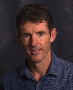 Samuel Naffziger is a Corporate Fellow at AMD responsible for technology strategy. He has been in the industry 30 years with contributions in power technology, processor architecture and circuit design, starting at Hewlett Packard, moving to Intel and then at AMD since 2006. He received the BSEE from the California Institute of Technology in 1988 and MSEE from Stanford in 1993 and holds 120 US patents in processor circuits, architecture and power management. He has authored dozens of publications and presentations in the field and is a Fellow of the IEEE.
Abstract: Datacenter solutions have been profoundly impacted with the advent of cloud computing and has been influencing the architecture trends of datacenter at large across all segments. In this presentation, we will discuss the key computing paradigms (e.g., warehouse scale computing) that underpin the cloud computing as well as some of the emerging trends (e.g., server less computing). We will highlight the CPU architecture advancements that will be needed to optimally address these paradigms and trends. In addition, we will also discuss the deployment of AI as well as massive growth of data is transforming cloud computing and driving changes to CPU architecture. We will also discuss how some of the foundational capabilities like security, power efficiency, quality of service etc. are impacted by the trends in the cloud computing.
 Sailesh Kottapalli is an Intel Fellow and Director of datacenter processor architecture. In this capacity, he leads the architecture for all the processors product lines at Intel targeted at the datacenter market including Xeon, Xeon-Phi, Xeon-SoC and Atom server product lines. He is also responsible for driving the architecture strategy and direction for computing needs in the datacenter. Previously, he was the lead architect for a number of generations of Xeon processor including NHM-EX, IVB server and Skylake server.
Abstract: Microsoft is building data centers with an FPGA in every server, creating the first Configurable Cloud. The FPGA is cabled between the NIC and the data center network, as well as being attached to the CPUs via PCIe. This architecture enables an FPGA-centric, rather than CPU-centric, computational model since all communication in and out of the server is first processed by the FPGA that handles common tasks without CPU involvement. Microsoft has deployed a diverse set of applications, including deep neural networks and software defined networking acceleration, across its Configurable Cloud. I will describe the Cloud, some of its applications, and their performance.
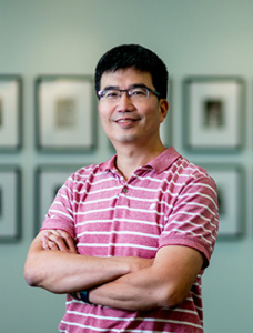 Derek Chiou is a Partner Group Hardware Engineering Manager at Microsoft where he leads the Azure team focused on FPGA eco-system, tools, and IP for data centers, and an adjunct associate professor in the Electrical and Computer Engineering Department at The University of Texas at Austin. Until 2016, he was an associate professor at UT. His research areas are novel uses of FPGAs, high performance computer simulation, rapid system design, computer architecture, parallel computing, Internet router architecture, and network processors. Before going to UT, Dr. Chiou was a system architect and lead the performance modeling team at Avici Systems, a manufacturer of terabit core routers. Dr. Chiou received his Ph.D., S.M. and S.B. degrees in Electrical Engineering and Computer Science from MIT.
Abstract: Thanks to the enormous progress and success of deep neural networks (DNNs), computer architecture research has been regaining its past “excitement” again recently: a lot of architectural proposals have been proposed for the accelerated execution of the training or inference of DNNs. Most of them have common architectural features: i.e., hardware-oriented, reconfigurable, domain-specific, and in/near-memory. This talk will try to give 1) insights on why they are happening now, 2) what are the recent findings in this movement, and 3) where this architectural innovation will be heading especially in the cloud computing context. This talk will also cover three such research examples that the lecturer developed or co-developed: 1) dynamically reconfigurable processor (DRP) developed by Renesas Electronics, 2) binary reconfigurable in-memory DNN accelerator (VLSI 2017), and 3) log-quantized and 3D-memory stacked DNN accelerator (ISSCC 2018).
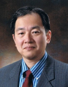 Masato Motomura received B.S. and M.S. in 1985 and 1987, respectively, and Ph.D. of Electrical Engineering in 1996, all from Kyoto University. He joined NEC central research laboratories in 1987, where he worked on various hardware architectures including string search engines, multi-threaded on-chip parallel processors, DRAM-FPGA hybrid systems, memory-based processors, and reconfigurable systems. During 2001 –2008, at NEC Electronics, he led business development of dynamically reconfigurable processor (DRP) that he invented. He was also a visiting researcher at MIT Laboratory for Computer Science from 1991–1992. Now a professor at Hokkaido University since 2011, his current research interests include reconfigurable and parallel architectures for deep neural networks and intelligent computing. He won the IEEE JSSC Annual Best Paper Award in 1992, IPSJ Annual Best Paper Award in 1999, and IEICE Achievement Award in 2011, respectively. He is a member of IEEE, IEICE, IPSJ, and EAJ.
Abstract: Traditional Von Neumann computing architectures, dominant for the last 70 years, is starting to give way to new paradigms. Specifically, the separation between computation and data storage is breaking down in several ways. For example, enablement of fast, cheap, non-volatile memory, accessed through a DRAM bus, is planned for current and future generations of CPU chipsets. A more far-reaching trend may be the placement of more powerful compute and storage elements in peripheral modules – in so-called “edge” applications – resulting in a more homogeneous distribution of compute and memory throughout a given ecosystem.
Both of these developments have been accelerated by the availability of new memory cell technologies, and new ways to integrate them into components. In this session, we will focus on the applicability of a given memory technology to a given compute/memory architecture. A wide range of both technologies and applications will be discussed. Technologies include 3DNAND, phase-change memory, various types of oxide-based resistive memory, and others. Applications include machine learning (specifically, the realization of the most common machine learning algorithms using analog compute-in-memory techniques), logic-in-memory, database functions such as map-reduce, and other applications. Our objective is to understand which attributes of each memory cell technology affect how well they fit into the different applications, the tradeoffs in designing components in these technologies for these applications, and the challenges that remain in bringing these components to the marketplace.
 Christopher Petti is an Engineering Fellow and Senior Director of Advanced Technology Development at Western Digital. He came to Western Digital as part of the acquisition of SanDisk in 2016. Dr. Petti has over 25 years of experience in a variety of semiconductor industries, including non-volatile memory, logic and SRAM technologies, flat-panel displays, and solar cells. In these fields, he has specialized in device physics, process integration, product architecture, and product engineering. Dr. Petti holds a B.S. in Physics from the Massachusetts Institute of Technology, and an M.S. and Ph.D. in Electrical Engineering from Stanford University. He is inventor or co-inventor on over 110 issued U.S. patents.
Abstract: Cloud computing requires many different interconnects. These links provide connectivity between and among CPUs, accelerators, memory, and switches; each link comes with its own distance and bandwidth requirements. Wireline transceivers are responsible for sending and receiving data from one chip to and from another, thus enabling required connectivity. The key specifications for such designs might include data rate, power consumption, area, and connection distance. The distance and data rate specifications, in particular, drive the choice of physical channel to be used for the connection, which in turn will drive requirements such as the equalization capabilities of the transceiver. For short chip-to-chip channels with limited frequency-dependent loss, simple transceivers with little or no integrated equalization are appropriate. For longer channels crossing backplanes and involving multiple transitions through connectors, complex transceivers with adaptive transmit and receive equalization are the right choice. As connection distances grow even longer, optical interconnect becomes an attractive option. In this talk, a framework for understanding serial link design will be presented, including a discussion of basic equalization strategies and key challenges. Next, several design examples will be presented, covering approaches to key classes of interconnect, from short reach channels to backplane channels to enabling highly integrated optical approaches. The talk will conclude with a discussion of emerging directions in this field.
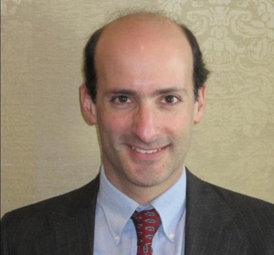 Daniel Friedman is currently a Distinguished Research Staff Member and Senior Manager of the Communication Circuits and Systems department of the IBM Thomas J. Watson Research Center. He received his doctorate from Harvard University in 1992 and subsequently completed post-doctoral work at Harvard and consulting work at MIT Lincoln labs, broadly in the area of image sensor design. After joining IBM in 1994, he initially developed field-powered RFID tags before turning to high data rate wireline and wireless communication. His current research interests include high-speed I/O design, PLL design, mmWave circuits and systems, and circuit/system approaches to enabling new computing paradigms. He was a co-recipient of the Beatrice Winner Award for Editorial Excellence at the 2009 ISSCC, the 2009 JSSC Best Paper Award (given in 2011), and the 2017 ISSCC Lewis Winner Outstanding Paper Award; he holds more than 50 patents and has authored or co-authored more than 75 publications. He was a member of the BCTM technical program committee from 2003-2008 and of the ISSCC international technical program committee from ISSCC 2009 through ISSCC 2016; he served as the Wireline sub-committee chair from ISSCC 2012 through ISSCC 2016. He has served as the Short Course Chair from ISSCC 2017 to the present and is a member of the SSCS Adcom since 2018.
Abstract: Heterogeneous system integration with advanced packaging technology plays important role in providing new and better system solution for various applications in semiconductor industry, including high performance computing. This course will discuss leading package technology innovations, power delivery and thermal challenges.
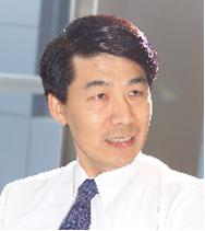 Douglas Yu (M’89-SM’06-F’13) is a Vice President of TSMC R&D in charge of interconnect and packaging technology development. He pioneered WLSI (Wafer-Level-System-Integration) technologies, including 3DIC/TSV (CoWoS), Integrated Fan-Out Wafer-Level-Packaging (InFO) and UBM-Free WL-CSP, for system integration of wide range products. Prior to that, Doug led the delivery of industry’s first advanced on-chip Cu/Low-K interconnects at TSMC’s 0.13 micron technology node. He received Ph.D. degree on Materials Science and Technology from Georgia Institute of Technology. Doug is an IEEE Fellow.
Abstract: These days, even non-technical people have declared that Moore’s law, namely, hardware performance improvement based on Si-transistor scaling, has almost ended. However, there seems to be no definite consensus on how to deal with this situation in the long term. As various solutions are proposed, those that are gaining a large amount of momentum involve specialized hardware to enhance the current integrated-circuit systems and seeking performance improvements in new directions such as quantum computing. In this presentation, we first describe the end of Moore’s law and its implication, which demands hardware specialization, and then introduce the basics of quantum computing to integrated-circuit engineers. Next, we focus on how the classical, integrated-circuit approach provides a path that leads to new directions including quantum computing, exemplifying digital-circuit based annealing hardware for quadratic unconstrained binary optimization.
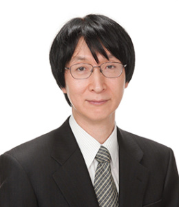 Hirotaka Tamura received his B.S., M.S., and Ph.D. degrees in electronic engineering from Tokyo University, Tokyo, Japan in 1977, 1979, and 1982. He joined Fujitsu Laboratories in 1982. After being involved in the development of different exploratory devices such as Josephson junction devices and high-temperature superconductor devices, he moved into the field of high-speed CMOS signaling in 1996 and got involved in the development of a multi-channel high-speed I/O for server interconnects. Since then, he has been working in the area of architecture- and transistor-level design for high-speed CMOS signaling circuits. Since 2014, he has been expanding his area to cover devices, circuits, and architectures for post-Moore-era computing. He is a Fellow of the IEEE.
Satellite Workshop
2018 Silicon Nanoelectronics Workshop
will be co-located with the Symposia on Sunday and Monday, June 17-18, 2018 at the Hilton Hawaiian Village.
2018 Spintronics Workshop on LSI
will be co-located with the Symposia at a date to be announced.

