Monday, June 18, 2018 – Device and Integration Technologies for Sub-5nm CMOS and Next Wave of Computing
Short Course:
Short Course:
Abstract: Silicon FinFET scaling is approaching its limit with gate length scaling limited by the tradeoff between short channel effects and channel mobility degradation. For beyond the 5nm node, new architectures are considered to overcome this limitation. The gate-all-around (GAA) structure is promising to further extend gate length scaling with enhanced short channel control. However, the channel cross-section area decreases, requiring multiple channels to compensate for the loss in current. The device structure should be optimized, considering the tradeoff between effective resistance and capacitance to meet the required performance and power requirements. Both horizontal and vertical nanowire transistors, as well as nanosheet transistors, are being evaluated as candidates for future nodes. In addition to the overall device architecture, different modules need development. Even if gate length scaling is electrically possible, processing challenges exist to enable multiple threshold voltages within the limitation of decreased space. Also, mobility enhancement is needed to compensate for the decrease in channel cross-section and reduced PFET channel stress from the reduced epitaxial source and drain volume with pitch scaling. New channel materials, such as SiGe and Ge can be considered to achieve this goal. With the introduction of new architectures and materials, reliability should also be evaluated. In summary, to continue scaling beyond the 5nm node, new architectures, such as GAA structures, may need to be introduced, along with the introduction of new materials and processing techniques.
 About Dong-Won Kim:
Dr. Dong-Won Kim is a Master of Logic Technology Development team, Semiconductor R&D Center, in charge of logic device development for 5nm and beyond 5nm node. He had worked in Samsung Electronics from 1989 to 1998 as a Process Engineer. After his Ph.D. study at UT Austin, in 2003, he rejoined Samsung Electronics. His research & development focus on the nano scaled device, 3 & 1 dimensional CMOS transistors, and 20nm, 14nm, 10nm, 7nm for logic device applications. He has authored or coauthored over 100 publications related to nano scale device for Logic application and is the holder of over 90 U.S. patents. He had severed on several IEEE conference technical committees including IEDM, SOI conference, ICICDT, VLSI-TSA and Silicon Nanoelectronics Workshop.
He received the B.S. and M.S. degrees from Korea University, Seoul, Korea in 1987 and 1997, respectively, and the Ph.D. degree at the University of Texas, Austin in 2003.
Abstract: MOL and BEOL interconnects have become the main determinants of chip performance, power and area degradation due to an increasing RC delay. Continued node scaling that follows Si must be MOL and BEOL interconnect-centric (Meindl et al, 2003). This short course will focus on the evolutionary and potential revolutionary innovations that will be required to further the technology beyond 7nm. In particular, the introduction of new materials and processes, and other system scaling strategies will be evaluated in light of their potential impacts on performance and reliability.
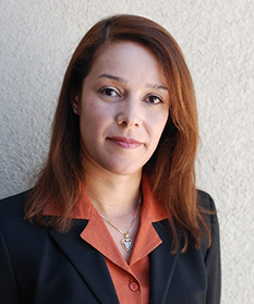 About Griselda Bonilla: Griselda Bonilla is currently a Senior Technical Staff Member (STSM) and Senior Manager of the Advanced Interconnect Technology group at IBM Research. Griselda leads a cross-functional team involved in the integration, scaling, and optimization of semiconductor materials, on-chip interconnects, and processes for use in the next generation of chips and electronic devices. In this role, she has a proven track record of successfully taking research concepts from the laboratory to early production. Her work has been rewarded internally with several technical accomplishments, including a Corporate Award in 2016, IBM’s highest technical recognition. She has authored or coauthored over 80 papers and presentations and has been issued over 30 patents.
Prior to this role, Griselda was responsible for extending IBM’s microelectronics technology and manufacturing leadership through innovations in materials, processes, and reliability methodology. This work lead to a detailed understanding of the impact of scaling and material properties on reliability performance of semiconductor devices and was responsible for setting Back-End-Of-Line (BEOL) interconnect materials roadmap for robust electrical and mechanical reliability. Since joining IBM, she has delivered technology solutions for multiple generations of CMOS technology used in respective IBM “P” and “Z” servers and miscellaneous ASIC products, including game processors.
Abstract: At 5nm design rules, atomic scale effects kick in on several levels: the band structures of Si and SiGe fins deviate from bulk properties, impacting transistor performance by about 10%. Further scaling makes transistor behavior even more sensitive to atomic scale changes in critical layer thicknesses, including fin/nanowire thickness changes as the current flows from source to channel and from channel to drain. We also explore different types of surface roughness due to plasma etch and lithography line edge roughness and its impact on transistor behavior. Quantum transport analysis suggests very non-intuitive engineering of surface roughness that can be transparent to the current flow for certain surface roughness patterns. The emerging role of atomic scale and quantum transport effects indicate a paradigm shift towards band structure driven transistor design. A key side effect of this is that the choice between different transistor architectures will come down to imperfections of different architectures and how these imperfections can be controlled and mitigated in high volume manufacturing environment. Atomic scale effects are inherently difficult to capture and quantify experimentally. Therefore, we use rigorous ab-initio physical approach to characterize such effects and extract guidelines for the future transistor design.
 About Victor Moroz: Victor Moroz received Ph.D. degree in Applied Physics from the University of Nizhny Novgorod in 1992 and joined a Stanford spin-off Technology Modeling Associates in 1995, which later became a part of Synopsys, connecting a design company to the manufacturing.
Currently Dr. Moroz is a Synopsys Fellow and Editor of Electron Device Letters, engaged in a variety of projects on analysis of advanced CMOS technology. Several facets of this activity are reflected in 100+ publications and 100+ granted and pending US patents.
Abstract: 3D integration is core technology for advanced devices. CMOS image sensor (CIS) uses 3D integration technology most effectively and has remarkably progressed for these years. In order to realize higher sensitivity and multi-functionality, many types of back-illuminated (BI) stacked CISs are currently in mass production.
This talk will focus on recent progress of 3D integration technology used in CIS devices, including
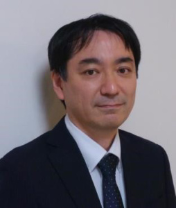 About Ryoichi Nakamura: Ryoichi Nakamura received B.S., and M.S. degrees from Tokyo Institute of Technology in 1994 and 1996 respectively. He has been working on DRAM, SRAM, and CMOS device and process development. He is currently involved in Device Development Division of Sony Semiconductor Solutions Inc. and recently he is engaging himself in the 3D stacked CMOS image sensor development.
Abstract: The information infrastructure is growing and becoming ubiquitous around us. Continuous connectivity, which we take for granted now, did not exist 10 years ago. This growth has been largely fueled by the scaling of the transistors which has allowed increased performance for comparable energy consumption and lower cost. Continuing growth further will demand a variety of electronic systems with different performance and energy efficiency requirements to satisfy a large set of functionality and cost needs.
The pace of innovation will like continue further as it is driven by technological needs. The scaling of the transistor will be influenced by fundamental physical limits of device switching. As these fundamental limits for traditional materials such as Si and SiGe, other materials could take their place. Further down the road, revolutionary devices that do not rely on simple charge states will likely be used. Devices which employ spin, exciton or plasmon states as the information carrier and state variable have already been proposed and are being actively investigated as replacements for the CMOS transistors.
This presentation will address several aspects of the quest for higher performance and/or lower energy consumption. We will review activities on 2D semiconductors for MOSFET applications. We will briefly discuss steep-slope concepts such as tunnel FETs and negative capacitance. We will explain how functional scaling can create an advantage by scaling circuits rather than devices. In this context, we will discuss spintronic majority gates and their potential for low energy operation. We will introduce the concept of quantum computing which promises to revolutionize computation through massive intrinsic parallelization.
 About Iuliana Radu: Iuliana Radu is Distinguished Member of Technical Staff at imec responsible for Beyond CMOS and Quantum Computing activities at IMEC. Beyond CMOS activities include work on novel device concepts including spintronics and wave computing and novel materials and their possible applications in the semiconductor industry. Quantum Computing activities includes work on qubit devices and the periphery circuits meant to control them. Prior to establishing the Beyond CMOS program at IMEC in 2013, she was a Marie Curie and FWO fellow at KU Leuven and IMEC. Her work at IMEC and KU Leuven included devices using the metal to insulator transition, ionic and electronic transport in functional oxides, and devices with graphene and other 2D materials.
Abstract: The R&D of AI devices is always led by computational algorithms that create new values and applications of AI systems. Recent AI devices tends to compete in their power/computational efficiency, but are not strongly oriented to pioneering new AI functions driven by hardware, due to the existence of wide gaps between information science (including software AI) and device engineering. In this lecture, the common representation for brain-morphic AI elements that could be shared in both the worlds of information science and device manufacturing will be introduced, to bridge the gap. This representation may give the participants important clues to re-define unit devices for brain-morphic AI computing; i.e. scalable 3D neural devices (not conventional logic and memory devices), towards reaching the technological singularity of AI.
About Tetsuya Asai: Dr. Tetsuya Asai is currently a professor at Hokkaido University. Born in Sapporo in 1969. Graduated with Doctor Degree of Engineering from Toyohashi University of Technology, Japan, in 1999. Visiting Professor of CEMS, University of the West of England, from 2004 to 2009. Member of System Device Roadmap committee of Japan (SDRJ) and IEEE International Roadmap for Devices and Systems (IRDS). Research interests are focused on intelligent integrated circuits and their computational applications, emerging research architectures, deep learning accelerators, and device-aware neuromorphic very large-scale integrations.
Abstract: Deep neural nets (DNNs) are gaining high momentum as evident by the number of commercially available deep learning accelerator products from multiple companies covering power constrained applications at the edge to thermally limited ones at the clouds. The focus of this talk will be on current and upcoming memory technologies needed to continue the momentum of DNNs. The presentation starts by reviewing memory use in contemporary DNNs. This will be followed by analyzing real life memory implementations in DNN accelerators from both industry and academia. Then, I will detail some of the ongoing and future memory technologies targeting DNN at all levels including compression/pruning schemes, data precision optimizations, compute in or near memory, 3D memories, and resilient memories. The talk will end with a summary and pointers to future areas of research.
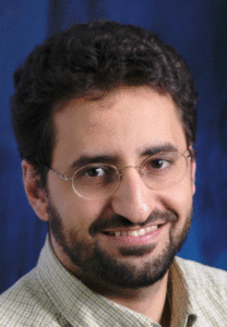 About Muhammad Khellah: Muhammad M. Khellah is a principal research scientist at Intel Labs. After obtaining his PhD from the University of Waterloo Canada in 1999, he joined Intel and was first involved in the design of L1/L2 caches for the Pentium microprocessor product line. He later joined Intel Labs where he currently leads research on low-power circuits and systems with particular focus on power management, resiliency, embedded memories, and machine learning. Dr. Khellah served as an associate editor for the IEEE TCAS-I, technical program co-chair for the 2014 IEEE/ACM ISLPED, and general co-chair for the 2016 IEEE/ACM ISLPED. He currently serves on the TPC of the IEEE ISSCC and as the special-sessions chair of IEEE CICC.
Abstract: Size and power constrained applications increasingly require sensing completely integrated down to the packaged integrated circuit level. Automotive driving assistance systems use mm-wave radars that have moved from discrete to single-chip transceivers, with antenna-on-packages for future miniaturization. Industrial automation and electric vehicles need form factor optimized magnetic sensors for detecting position, speed, and current. This paper will review these and other applications that are driving this integrated sensor trend, show example systems, and ultimately drive into requirements on the underlying technology, whether these leverage the speed of advanced CMOS technologies, introduce custom devices, and/or use novel packaging techniques.
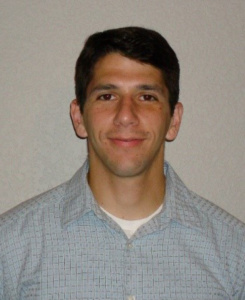 About Brian Ginsburg: Brian Ginsburg received his S.B., M.Eng., and Ph.D. degrees from the Massachusetts Institute of Technology. He joined Texas Instruments, Dallas, Texas in 2007 working in its wireless terminals business unit and Kilby research labs. He is the systems manager of TI’s Radar and Analytics Processors organization, developing mm-wave sensors for automotive and industrial applications. He serves on the ISSCC and VLSI Circuits Symposium Technical Program Committees.
2018 Silicon Nanoelectronics Workshop will be co-located with the Symposia on Sunday and Monday, June 17-18, 2018 at the Hilton Hawaiian Village.
2018 Spintronics Workshop on LSI will be co-located with the Symposia at a date to be announced.