logo

Plenary, Panel Sessions and Luncheon

The plenary sessions for Technology and also Circuits will each consist of two distinguished industry leaders to describe recent advances and new challenges related to VLSI Technology / VLSI circuits, technology and applications.

The Technology Plenary will be held Tuesday morning, June 14. The Circuits Plenary Session will be held Wednesday morning, June 15.

VLSI Technology and Circuits Symposium evening Panel Sessions are well known for their selection of timely topics and enthusiastic discussions on interesting and provocative topics with technical leaders on the panel to provide all conference attendees an opportunity to participate in the discussions and mix with other attendees and in the audience.

The VLSI Technology Panel Sessions will be held on Tuesday evening, June 14. The Circuits Panel Sessions will be held on Thursday evening, June 16.

Tuesday, June 14

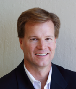
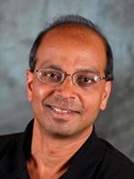
“The Age of Sensors – How MEMS sensors will enable the next wave of new products”, Stephen Lloyd, VP of Engineering and New Product Development, InvenSense, Inc.

This talk will cover the evolution of MEMS sensors from research into the main stream, and how a new generation of sensors will drive several major technology inflections.

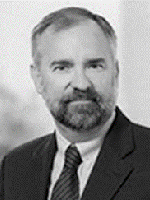
Lloyd

Stephen Lloyd is the Vice President of Engineering and New Product Development for InvenSense. Inc., where he is responsible for Advanced Sensor Technology and all Sensor HW Product Development, a position he has held since December 2008. Steve is focused primarily on highly integrated MEMS motion sensors for consumer applications, such as cell phones, cameras, gaming, wearables, drones, and IOT.  Recent product developments now include automotive and industrial motion sensors, as well as MEMS microphones and other new sensor technologies.

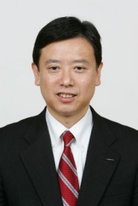
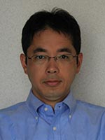
“Intelligent Mobility realized through VLSI”, Takao Asami, Senior Vice President, Nissan

Since the first introduction of a microprocessor into an automobile in 1970’s, the world has been witnessing its dramatic growth as well as its contribution to all aspects of vehicle performance.  At the same time, as the global demand for personal mobility grows continuously, the automotive industry needs to accelerate the development of solutions for the social problems such as environment, energy security, traffic accidents, and urban traffic congestions.  To address these issues, Nissan pursues the ultimate goal, “Zero Emission” and “Zero Fatality”, through the vehicle electrification and the vehicle intelligence.  The electric vehicle is a symbol of electrification that components are fully electrically powered and controlled. Autonomous driving technologies are examples of vehicle intelligence, such as advanced sensing technologies, dynamic driving context interpretation, vehicle maneuver planning and its control.

This session provides an overview of VLSI’s contribution for enhancing vehicle electrification and vehicle intelligence and its perspective of the future mobility system.

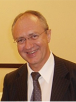
AsamiTakao Asami is the Senior Vice President for Research and Advanced Engineering at Nissan, and also the Alliance Global Vice President for the Renault Nissan Alliance. He joined Nissan in 1981 after graduating from the University of Tokyo. He also holds Master of Science in Electrical Engineering from the University of Southern California.  Mr. Asami spent 15 years working through the organization before moving to Nissan Technical Centre North America in Detroit, in the United States, in 1995.  Six years later, as Nissan launched its IT Engineering Department, he returned to Japan to lead the team and drive forward in developing the company’s expertise. In April 2006 he transferred to Nissan’s Alliance partner, Renault. Three years later he was back at Nissan as the Corporate Vice President in charge of the Nissan Research Center.  He was appointed as Senior Vice President in charge of Technology Planning and Advanced Engineering in April 2013 and was appointed to current role in April 2014.

Wednesday, June 15

To Be Announced

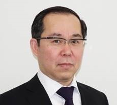
“Accelerating the Sensing World through Imaging Evolution”, Tetsuo Nomoto, Vice President and Senior General Manager, SONY

The evolution of CMOS Image Sensors (CIS) and the future prospect of a “sensing” world utilizing advanced imaging technologies promise to improve our quality of life by sensing anything, anywhere, anytime. Charge Coupled Device image sensors replaced video camera tubes, allowing the introduction of compact video cameras as consumer products. CIS now dominates the market for digital still cameras created by its predecessor and, with the advent of column-parallel ADCs and back-illuminated technologies, outperforms them. CIS’s achieve better signal to noise ratio, lower power consumption, and higher frame rate. Stacked CIS’s continue to enhance functionality and user experience in mobile devices, a market that currently comprises over one billion new image sensors per year. CIS imaging technologies promise to accelerate the progress of sensing world by continuously improving image quality, extending detectable wavelengths, and further improving depth resolution and temporal resolution.

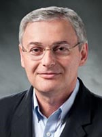
NomotoTetsuo Nomoto received the B.S. and M.S. degrees in applied physics from Tohoku University, Sendai, Japan, in 1988 and 1990, respectively. In 1990, he joined Olympus Optical Corporation, Nagano, Japan, where he was involved in the development of charge modulation device image sensors. He joined Sony Corporation, Kanagawa, Japan, in 2001, where was engaged in the development of CMOS active pixel sensors. From 2015, he has been responsible for image sensor business for mobile application.

Tuesday, June 14, 8:00 pm – 10:00 pm

“More Moore, More than Moore, or Mo(o)re Slowly”
Moderator: Subu Iyer, University of California Los Angeles

Abstract
Over the past 50 years, rapid advancement of fabrication technology has allowed doubling the number of transistors in VLSI components every two years. This trend has continuously enabled new system features that had been previously impractical if not impossible. As a result of this, the growth of the global semiconductor market has been predominantly fueled by technology scaling in what can sometimes be referred to as a “more of the same is good enough” paradigm. As technology scaling slows down, this dynamic is changing and it is unclear what will drive future growth. Is the industry going to continue a similar path through introduction of new devices and 3D integration? Or is the end of silicon scaling the end of brute force large-scale integration? If that is the case, what is the value of sensor and system integration? Can they generate enough demand to drive growth at a rate comparable to silicon integration? And what is the role of circuit innovation in this environment? One might argue that the “more of the same is good enough” attitude of the past few decades has been a major hindrance for emergence and adoption of many promising ideas at the circuit level? Is the end of scaling a blessing in disguise for the talented circuit designer who would love to tackle a more constrained problem? Renowned experts will attempt to answer these very important questions in this panel.

Circuits Panel

iyer-subramanianSubramanian Iyer teaches at the University of California at Los Angeles. Prior to that he was an IBM Fellow. Over his career, he has worked the area of devices, processes, integration, embedded memory 3D integration, advanced packaging and system integration. His website is chips.ucla.edu. He is an IEEE Fellow and received the IEEE Daniel Noble award in 2012.
de-vivekVivek De is an Intel Fellow and Director of Circuit Technology Research in Intel Labs. He is responsible for providing strategic technical directions for long term research in future circuit technologies and leading energy efficiency research across the hardware stack. He has 240 publications in refereed international conferences and journals and 205 patents, with 30 more patents filed. He received an Intel Achievement Award for his contributions to an integrated voltage regulator technology. He received a PhD in Electrical Engineering from Rensselaer Polytechnic Institute, Troy, New York. He is a Fellow of the IEEE.
lu-nickyAs a researcher, designer/architect, entrepreneur and chief executive, Dr. Nicky Lu has dedicated his career to the worldwide IC design and semiconductor technology over 30 years. He is CEO and Founding Chairman of Etron Technology, Inc. and co-founded several technical companies which are public today. He has MS/Ph.D. degrees from Stanford University, received an IBM Corporate Award and IEEE Solid-State Circuits Technical Field Award. He is an IEEE Fellow and a member of National Academy of Engineering, and serves as Chair of Taiwan Semiconductor Industry Association.
patton-garyDr. Gary Patton is the Chief Technology Officer and Senior Vice President of Worldwide Research and Development at GLOBALFOUNDRIES where he is responsible for GLOBALFOUNDRIES’ semiconductor technology R&D roadmap, operations, and execution. Prior to joining GLOBALFOUNDRIES, Dr. Patton was the Vice President of IBM’s Semiconductor Research and Development Center - a position that he held for eight years where he was responsible for IBM’s semiconductor R&D roadmap, operations, execution, and technology development alliances across multiple locations.  Dr. Patton is a well-recognized industry leader in semiconductor technology R&D with over 30 years of semiconductor experience. Dr. Patton received his B.S. degree in electrical engineering from UCLA and his M.S. and Ph.D. degrees in electrical engineering from Stanford University. He is a Fellow of the IEEE, a member of the IEEE Nishizawa Medal Awards Committee, has co-authored over 70 technical papers and given numerous invited keynote and panel talks at major industry forums.
skotnicki-thomasThomas SKOTNICKI is the STMicroelectronics Company Fellow and Technical Vice-President in charge of Disruptive Technologies at STMicroelectronics Crolles, France. In 2007, he received the title of Professor from the President of Poland, and recently has been appointed the Director of CEZAMAT (Research Consortium) in Warsaw, Poland. The focus of his program at STMicroelectronics is on Low Power / Low Variability for 28nm and beyond CMOS, on innovative device structures, new memory concepts and cells, and on integration of new materials for CMOS. From 2010 he has extended the scope of his program to include Energy Harvesting for autonomous Low Power systems and devices. He holds more than 80 patents on new devices, circuits and technologies. He has presented over 50 Invited Papers and Short Course Lectures, (co-) authored about 350 scientific papers (review based), and several book chapters in the field of CMOS and Energy Harvesting. From 2001 to 2007, he served as Editor for IEEE Transactions On Electron Devices. He has been teaching at EPFL (Lausanne, Switzerland) and SUPELEC (Rennes, France), and has supervised and led to successful defence 26 PhD theses. He has been serving in numerous Conference Program and Executive Committees (IEDM, VLSI, ESSDERC, ECS, SNW, IWJT), Academia Advisory Boards, Governmental Expert Commissions, R&D Program Steering Committees, IEEE Award Committees (JJ Ebers and Frederik Philips), and ITRS (who has been using his/his team software MASTAR for 12 consecutive editions). He is an IEEE Fellow and SEE Senior Member.
vardaman-janE. Jan Vardaman is president and founder of TechSearch International, Inc., which has provided analysis on technology and market trends in semiconductor packaging since 1987. She is co-author of How to Make IC Packages (published in Japanese by Nikkan Kogyo Shinbunsha), a columnist with Printed Circuit Design & Fab/Circuits Assembly Magazine, She is an IEEE CPMT distinguished lecturer and the author of numerous publications on microelectronics market and technology trends. She is a member of IEEE CPMT, IMAPS, MEPTEC, and SEMI. She served two terms on the CPMT Board of Governors. She served on the NSF-sponsored World Technology Evaluation Center study team involved in investigating electronics manufacturing in Asia and on the U.S. mission to study manufacturing in China. Before founding TechSearch International, she served on the corporate staff of Microelectronics and Computer Technology Corporation (MCC), the electronics industry’s first pre-competitive research consortium. She received her B.A. in Economics and Business from Mercer University in Macon, Georgia in 1979 and her M.A. in Economics from the University of Texas at Austin in 1981.

Tuesday, June 14
8:00 p.m. – 10:00 p.m.

“How Moore’s Law, Industry Consolidation, and System Trends are Shaping the Memory Roadmap”
Moderators:  Gary Bronner, Rambus and Fred Chen, Winbond

Preliminary questions for the panel:

  • Moore’s Law – are we at the end for the scaling of memories?  What’s the metric of interest?  Capacity? Design Rule? Cost? Performance? Power/Energy Efficiency?
  • Why do we need anything beyond DRAM and Flash? What is the impact of slowing DRAM cost reduction on their use in products and systems?
  • For Flash Technology
  • Will conventional 2D NAND survive or 3D NAND completely replace it?
  • What are the technical limits for 3D NAND?  When does it stop scaling?
  • For DRAM Technology
  • Will the introduction of compact, high BW memory (HBM) lead to a chance in memory hierarchy)?
  • Where and when will 3D stacked memory become a volume product?
  • Where and when will new/emerging memory technology first enter the market? What is the customer adoption status?
  • How would the memory hierarchy change with the introduction of SCM (storage class memory)?
  • Industry consolidation – how many vendors does the world need?

Abstract:

The roadmap for memory, both DRAM and Flash, has historically been driven by a self-fulfilling prophecy – memory cost must drop 35% / year on a cost per bit basis.  Moore’s law drove this exponential decrease in cost and increase in memory density for over 3 decades.  But the last decade has seen interesting modifications to this historical trend.  The emergence of NAND Flash memory led to even faster drops in price, with NAND now 16x cheaper than DRAM on a cost/bit basis.  DRAM scaling limits are causing DRAM density improvement to slow and the price gap to widen.   NAND Flash continues on a classical price/density roadmap but its performance is not sufficient to replace DRAM.   Current systems and applications are facing a “Memory Wall” – cheap Flash bits don’t meet CPU performance needs while DRAM bits are no longer cheap enough to meet the capacity needs of multicore CPUs.  This has triggered a burst of innovation at all levels – technology, system, and software, creating a myriad of possibilities to be considered.

This panel will debate the technology roadmaps for DRAM, FLASH, SCM (storage class memory) and eNVM (embedded Non Volatile Memory) in light of the fundamental problems around memory cost, performance, and power.   Can any of the emerging NVM technologies provide compelling solutions to current computer system and application needs?  Which industry will drive the new memory technology – data centers or mobile chip vendors?  What memory (or combination of memories) gives the lowest total cost of ownership?  How will computer systems handle new levels of memory hierarchy?  How does industry consolidation and the emergence of new players in the memory industry affect the roadmap? These and other questions raised from the audience will be addressed by a distinguished panel of experts from industry.   It is a most interesting time to be involved in the memory world!

Memory Panel

bronner-garyGary Bronner is Vice President of Rambus Labs, where he is responsible for his company’s long term research in memory devices and systems.  Prior to joining Rambus in 2006, he was at IBM where he was responsible for the development of many generations of DRAM technology.  He is author or co-author of over 80 issued US Patents along with numerous journal and conference publications.  He received his ScB degree from Brown University and MS and PhD degrees from Stanford University.  He is a Fellow of the IEEE.
chen-frederickDr. Frederick Chen received his Ph.D. in Applied Physics from Cornell University, after demonstrating the first artificial dielectric diffractive optical element at a visible wavelength. After receiving his Ph.D., he worked at Intel's Mask Operations, developing advanced photomasks for the 0.25 um to 45 nm nodes as well as for EUV and double patterning. In 2005, he moved to Taiwan's Industrial Technology Research Institute, where he worked on developing and modeling advanced phase change memory structures and later HfO2-based resistive memory. At ITRI, he and his patterning team also developed self-trimming double patterning, which was implemented in the cross-spacer phase change memory published at IEDM 2007. He is currently at Winbond Electronics, where he is helping to improve RRAM reliability and establishing the filamentary RRAM model.   
borkar-shekharShekhar Borkar is an Intel Fellow, an IEEE Fellow, and Director of Extreme-scale technologies at Intel Corporation. He served as the TPC chairman of VLSI Circuit Symposium in 2002, and as the conference chairman in 2004. Shekhar was an adjunct faculty at Oregon Graduate Institute, taught graduate course on VLSI design for more than 10 years. His research interests are low power, high performance digital circuits, high speed signaling, and system level optimization. Shekhar holds M.Sc. in Physics from University of Bombay in 1979, and MSEE from University of Notre Dame in 1981.
kono-takashiTakashi Kono received the B.S. and M.S degrees in electronic engineering from University of Tokyo, Tokyo, Japan, in 1992 and 1994, respectively. In 1994, he joined Mitsubishi Electric Corporation. From 1994 to 2002, he was engaged in the research and design of DRAMs from 64Mb to 512Mb including synchronous DRAMs and DDR/DDR2 DRAMs. After transferring to Renesas Technology Corporation in 2003, he worked on the development of low-power pseudo-SRAM and high-density flash memories. He is currently with Renesas Electronics Corporation, where he has been supervising the development of advanced embedded Flash memory for high performance Flash MCUs. Since 2014, he has been serving for memory sub-committee of ISSCC.
lee-jaejinJaejin Lee received the B.A degree at Physics from Seoul National University in Seoul, Korea in 1986. He has been working as DRAM design engineer for over 25 years at SK Hynix and he was always on the edge of the first developments of all the types of DRAMs. In recent years he completed the development of HBM1 on general responsibility and now he is leading Design Innovation Lab to envision and realize the concepts of future memories as a Research Fellow at SK Hynix. He has over 50 US patents.
lim-junheeJunhee LIM worked at Samsung for the past 15 years, participating the DRAM research and developing program from 5x nm to 2x nm technology node and late managing the design and fabrication of the peripheral transistor of DRAM. Since 2015, he has been involved in developing Vertical NAND Flash device at the R&D center in Samsung Electronics. He earned his B.S. in electrical engineering from the Seoul National University, Korea.
sandhu-gurtejGurtej S. Sandhu is Senior Fellow and Director of Advanced Technology developments at Micron Technology, Inc. In his current role, he manages the Advanced Memory Technologies Roadmap and forward looking Research & Development at Micron. He received degree in electrical engineering at the Indian Institute of Technology, New Delhi and a Ph.D. degree in physics at the University of North Carolina, Chapel Hill, in 1990. Dr. Sandhu then joined Micron Technology, where he has been in a number of engineering and management roles responsible for process technology development, pilot manufacturing and transfers to manufacturing. He has been associated with microelectronics technology for over 20 years and has pioneered several process technologies which are currently employed in mainstream semiconductor chip manufacturing. Moreover, he was involved with introduction of a number of Atomic Layer Deposition (ALD) based processes and innovative patterning techniques for memory chip technology. Dr. Sandhu has authored over 35 technical papers and several hundred issued U.S. patents. Dr. Sandhu is Fellow of IEEE.
sprinkle-robRob Sprinkle is a Technical Lead in Google's Data Center Infrastructure Advanced Technology Team. He is responsible for working with established and emerging memory technology companies to track and influence strategic technical directions, and internally to determine best uses of custom and emerging memory technologies and designs in the data center infrastructure. Previously he was the Technical Lead for the concept and hardware design of Google's first custom NAND Flash storage tier, and is a recipient of Google's second highest corporate recognition award. Prior to 2006, he was a PCB and ASIC/FPGA designer/manager at Teradyne. He received a BSEE from the Virginia Military Institute and has been issued numerous patents with others pending.

Thursday, June 16
8:00 p.m. – 10:00 p.m.

“Top Circuit Techniques: Life With and Without Them”
Organizer: Dejan Markovic, University of California, Los Angeles and Kenichi Okada, Tokyo Institute of Technology
Moderator:   Un-Ku Moon, Oregon State University

Panel consisting of experts from different areas will provide a review of the highest-impact circuit techniques, and give examples of how these techniques brought significant system advances. After the opening statement from each of panelists, limited to one technique, audience can debate to gauge the impact of those techniques. At the end of the panel discussion, everyone can join to vote the top three circuit techniques in 2016.

Panelists
Takahiro Miki, Renesas
Marvin Chang, Nat’l Chiao Tung University/ITRI
Asad Abidi, University of California, Los Angeles
Ippei Akita, Toyohashi University
Muhammad Khellah, Intel
Adrian Tang, Jet Propulsion Lab
Andreas Burg, EPFL
Cyrus Afghahi, Broadcom


It’s All a Common Platform – How Do I Build a Differentiated Product?”

Organizers: Fatih Hamzaoglu Intel and Masanori Hashimoto, Osaka University
Moderator:  Ajith Amerasekera, Texas Instruments

Chip industry has been very competitive in recent years as semiconductor Foundry, Memory suppliers, IP developers, and EDA tools have diminished to few players. With very tight TTM (Time to Market) and cost requirements, vendors have limited value options to add to their products to differentiate from competition. The panelists will discuss how innovation, software hardware co-design, cost vs. performance optimization, user interface and other factors can differentiate their products even with common infrastructure.

Panelists
Hugh Mair, MediaTek
Robert Aitken, ARM
Steve Young, Xilinx
Suk Lee, TSMC
Hoi Jun Yoo, KAIST
Takashi Kono, Renesas
Mark Doran, Intel

MaharbizHighRes1


“Cyborg Insects & Other Things; Building Interfaces Between the Synthetic & the Multicellular”
Speaker:  Michel Maharbiz, University of California, Berkeley

As the computation and communication circuits we build radically miniaturize (i.e. become so low power that 1 pJ is sufficient to bang out a bit of information over a wireless transceiver; become so small that 500 µm^2 of thinned CMOS can hold a reasonable sensor front-end and digital engine), the barrier to introducing these types of interfaces into organisms will get pretty low. Put another way, the rapid pace of computation and communication miniaturization is swiftly blurring the line between the technological base that created us and the technological based we’ve created. In this talk, I’ll give an overview of recent work in my lab that touches on this concern. Most of the talk will cover our ongoing exploration of the remote control of insects in free flight via implantable radio-equipped miniature neural stimulating systems.; recent results with neural interfaces and extreme miniaturization directions will be discussed. If time permits, I will show recent results building extremely small neural interfaces we call “neural dust,” work done in collaboration with the Carmena, Alon and Rabaey labs.