VLSI Circuits Short Courses – 2
- Home
- VLSI Circuits Short Courses – 2
Tuesday, June 14, 2016
Short Course: Circuit Design in FinFET, FDSOI and Advanced Memory Technologies
Designers are using FinFET transistors in the latest generation of processors to boost performance and reduce area. However, these transistors come with their own set of unique design challenges. In the future, as design dimensions continue to shrink and transistor structures evolve, these challenges are rising to become limitations on performance and reliability. This short course will review the design considerations and reliability concerns associated with FinFET transistor process technologies. Then it will chart processor performance, power, and area across the last few process technologies and project into the future to predict what the next generation of processors is likely to achieve.
About Jim Dodrill
 Jim Dodrill is a Senior Principal Design Engineer in the Advanced Products Division of the Physical Design Group at ARM in Austin, TX. He is responsible for developing new standard cells and related methodologies in advanced process technologies that improve the power, performance, area, and yield possible with ARM Artisan© Physical IP, especially when used to implement ARM CPU and graphics cores. His recent work has focused on synchronizer design, on-chip variation, and soft error tolerance. Jim earned a Bachelor of Science in Electrical Engineering degree from Oklahoma State University and a Master of Science in Electrical Engineering and Computer Science degree from Duke University. His experience spans the range from custom transistor level design to full SOC chip tape-out and CAD enablement for companies including Texas Instruments, Ross Technology, and Analog Devices.
The introduction of finFET in 22-nm CMOS has accelerated foundry finFET offering with fabless 16/14-nm designs already in early production after a short-lived 20-nm planar node. With continued consumer demand for mobile SoCs, the readiness of finFETs could not be timelier because the superior short-channel control realized in a finFET prolongs substantial reduction in digital power with device area scaling. As SoC technology development remains dictated by logic and SRAM, designers of analog/mixed-signal subsystems must adapt to new design constraints. We attempt to summarize the fundamental challenges and considerations when porting common analog/mixed-signal building blocks to finFET. At 16/14 nm, designers deal not only with finFET implications but continue to be impacted by recent technology elements such as mechanical strain, high-permittivity gate dielectrics and metal gate, multiple patterning, and an increasingly complex middle-of-line.
About Dr. Alvin Loke
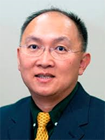 Dr. Alvin Loke received a B.A.Sc. in engineering physics from the University of British Columbia, and M.S. and Ph.D. in electrical engineering from Stanford. He worked on CMOS process integration for several years at HP Labs and on assignment at Chartered Semiconductor. Since 2001, he has been designing circuits for a variety of wireline links and addressing next-generation CMOS analog/mixed-signal concerns at Agilent and Advanced Micro Devices in Fort Collins, CO, and most recently at Qualcomm in San Diego, CA. He has authored several dozen publications and holds 17 US patents. Alvin has served as Technical Program Committee member of CICC, IEEE Chapter Chair, Guest Editor of the IEEE Journal of Solid-State Circuits, and IEEE Distinguished Lecturer.
Ever-increasing demand for computing power and energy efficiency in modern SoCs continues to drive logic technology scaling. The introduction of 3D FinFET transistor in 22nm CMOS logic process has enabled a path forward to continued process and voltage scaling by delivering superior short channel control and lower threshold voltage variation relative to bulk planar CMOS. These key characteristics have benefited the designs of 22nm and 14nm/16nm embedded memories, allowing continued improvements in density, power and performance. The new features in FinFET technology also bring challenge and consideration to embedded memory design. More than ever, the co-optimization between process technology and circuit assist techniques are required in order to deliver dense and low-power memory operation. In this talk, we will focus on: (1) embedded memory scaling trend and challenge, (2) key considerations for embedded memory design with FinFET transistor and advanced interconnect, (3) circuit techniques to address design and process challenges in FinFET technology. We will discuss these topics considering recent advances in FinFET CMOS technologies and design techniques.
About Yih Wang
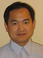 Yih Wang received his B.S. degree in Electrical Engineering from National Tsing Hua University, Hsinchu, Taiwan, and the M.S. and Ph.D. degrees in electrical and computer engineering from University of Florida, Gainesville. From 1999 to 2001, he was the Pittman-Eminent Scholar Predoctoral and Postdoctoral Fellow at University of Florida. He joined Intel Portland Technology Development in 2001. Since then, he has worked on the development of 90nm and 65nm standard-cell library for high-performance CPU, and a variety of low-power and high-speed embedded memory designs in 65nm to 14nm CMOS logic technologies. He is currently a senior principal engineer in logic technology development group. He has received three Intel Achievement Awards for his contributions on embedded memory technology development. He has authored and co-authored more than 35 journal and conference publications and has 28 issued and pending U.S. patents. He is a senior member of the IEEE.
The demand for high performance and high density NAND flash memory has increased as storages such as solid state drive(SSD) and mobile storage (eMMC, UFS) require more density and higher performance. In order to meet this demand many efforts have been tried to shrink down die size and to improve performance and reliability. However, 2D NAND Flash is facing a shrinking limit because of the increased cell-to-cell interference and patterning difficulties caused by scaling down. To overcome these limitations, many researchers have developed 3D-stacking technologies for long time. Recently, NAND Flash memory companies have been launching 3D NAND Flash, especially, Samsung succeeded in developing the third generation 3D V-NAND flash. Due to 3D V-NAND’s superior performance and reliability to 2D NAND Flash, 3bit/cell 3D V-NAND flash becomes able to meet the reliability requirement of Data center and Enterprise SSD, which is possible with 2bit/cell 2D NAND Flash. This talk will, therefore, cover the enabling technologies and improvement of 3D V-NAND flash in mobile storage and high reliability SSD demanding high density memory.
About Woopyo Jeong
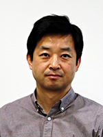 Woopyo Jeong is currently working for Samsung Electronics as a principal engineer. Woopyo Jeong received the B.S. and M.S. degrees in electrical engineering from Yonsei University, Seoul, Korea, in 1991 and 1993, respectively. In 1993, he joined Samsung Electronics, where he was engaged in research and development for DRAM. He received the Ph.D. degree in electrical and computer engineering from Purdue University, West Lafayette, IN, USA, in 2004. His study was sponsored fully by Samsung Electronics. After he graduated from Purdue University, he rejoined DRAM design team where he developed mobile DRAM as a project leader from 2004 to 2007. He moved to NAND Flash memory design team in 2007 and he has currently been involved in development 3-D Vertical NAND Flash as a project leader since 2013.
Fully Depleted Silicon on Insulator (FD-SOI) is one of the alternatives that permits today to follow the More Moore law of CMOS integration for the 28nm node and beyond, while still dealing with fully planar transistors. Numerous presentations have presented over the several last years the benefits of this technology for an energy efficient integration of digital signal processing cores. This talk will focus on the benefits of FD-SOI technology for analog/RF/millimeter-wave and high-speed mixed signal circuits, by taking full advantage of wide voltage range body biasing tuning. For each category of circuits (analog/RF, mmW and high-speed), concrete design examples are given in order to highlight the main design features specific to FD-SOI.
About Andreia Cathelin
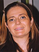 Andreia Cathelin started her electronic studies at the Polytechnic Institute of Bucarest, Romania and graduated from the Institut Supérieur d’Electronique du Nord (ISEN), Lille, France in 1994. In 1998 and 2013 respectively, she received PhD and “habilitation à diriger des recherches” (French highest academic degree) from the Université de Lille 1, France.Since 1998, she has been with STMicroelectronics, Crolles, France, now in Embedded Processing Solutions Segment, Technology R&D, as Senior Member of the Technical Staff. Her major fields of interest are in the area of RF/mmW/THz systems for communications and imaging.
Andreia is serving in several IEEE conferences and committees. She has been active at ISSCC since 2011: in 2011 as TPC member, RF sub-committee chair from 2012 to 2015, and is Forums Chair and member of the Executive Committee for ISSCC2016. She is member of several Technical Program Committees: VLSI Symposium on Circuits since 2010 – currently serving as officer and ESSCIRC since 2005. Since September 2013, Andreia is on the Steering committee of ESSCIRC-ESSDERC conferences, currently serving as Chair. She has authored or co-authored 100 technical papers and 4 book chapters, and has filed more than 25 patents. Andreia is a co-recipient of the ISSCC 2012 Jan Van Vessem Award for Outstanding European Paper and of the ISSCC 2013 Jack Kilby Award for Outstanding Student Paper; as well as winner of the 2012 STMicroelectronics Technology Council Innovation Prize. She is an elected member of the IEEE SSCS Adcom for the term January 2015 to December 2017.
Ultra-thin body and BOX fully-depleted SOI technology is an attractive platform for energy-efficient design, without major changes in the bulk-CMOS design infrastructure. Good control of short-channel effects with thin transistor body offers a possibility to operate at low supply voltages. Thin buried oxide provides threshold tuning via body bias. This presentation will focus on the UTBB FDSOI technology features and options, and highlight similarities and differences from bulk CMOS. A particular attention will be paid to SRAM design options available by the use of different well structures and bias voltages. Ideas for supply regulation and back-bias generation will be discussed and the talk will be supported by some measurement data in 28nm FDSOI technology.
About Borivoje Nikolić
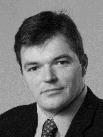 Borivoje Nikolić is the National Semiconductor Distinguished Professor of Engineering at the University of California, Berkeley. He received the Dipl.Ing. and M.Sc. degrees in electrical engineering from the University of Belgrade, Serbia, in 1992 and 1994, respectively, and the Ph.D. degree from the University of California at Davis in 1999. His research activities include digital, analog and RF integrated circuit design and VLSI implementation of communications and signal processing systems. He is co-author of the book Digital Integrated Circuits: A Design Perspective, 2nd ed, Prentice-Hall, 2003.
For work with his students and colleagues he has received the best paper awards at the IEEE International Solid-State Circuits Conference, Symposium on VLSI Circuits, IEEE International SOI Conference, European Solid-State Device Research Conference, European Solid-State Circuits Conference, S3S Conference and the ACM/IEEE International Symposium of Low-Power Electronics. In 2014-2015, he was Distinguished Lecturer of the IEEE Solid-State Circuits Society.
Satellite Workshop
2016 Silicon Nanoelectronics Workshop
will be co-located with the Symposia on Sunday and Monday, June 12-13, 2016 at the Hilton Hawaiian Village.
2016 Spintronics Workshop on LSI
will be co-located with the Symposia at a date to be announced.
