“Inflections in VLSI Technologies – Cloud & Beyond”
I. Cloud Computing
“Inflections in VLSI Technologies – Cloud & Beyond”
I. Cloud Computing
While some aspects of historical technology scaling may be reaching precarious plateaus, there has been no lack of new ideas from the ‘electrons and holes’ standpoint for looking beyond the conventional. Fully depleted transistors of both the planar and FinFET variety are now in the mainstream at the 14nm node and one can envision concepts that overcome critical pinch points for continued improvements in density, power, and performance for some generations beyond 7nm.
Additionally there is more to system-level performance than advances in transistors. Considerable enhancements in high-performance computing throughput can be accomplished with specialized hardware accelerators (FPGAs and GPUs) employed within a given transistor technology closely attached to the processor core. With the advent of the Cognitive Computing Era and the widespread use of Data Analytics, further significant improvements in System Performance can be obtained by exploiting the error resilience of these applications to technology, circuit, architecture and algorithmic errors.
Between continued transistor-level innovation in future nodes, and the addition of hardware-based application-specific accelerators and Approximate Computing techniques, the end of system performance improvements is nowhere in sight.
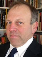 Terence Hook has worked on CMOS and bipolar and BiCMOS technologies at IBM in Burlington, Vermont, and East Fishkill and Albany, New York. He did his undergraduate work at Brown University and his PhD at Yale University in electrical engineering. While at IBM he has been instrumental in developing technologies from the micrometer to the nanometer level, most recently working with IBM’s partners at the Albany Nanotech center, focusing on FDSOI, FinFETs, and device options beyond that. Some of his sideline special interests include plasma charging damage and transistor matching. He has authored some 70 or papers and holds more than 100 patents.
Enormous data transmission urges optical interconnections to be implemented in rack to rack, board to board, and chip to chip communications. In future high bandwidth interconnections, optical I/Os will have to be densely integrated and compact because they should be mounted in the immediate vicinity of LSIs to save the power consumption used for the electric interconnection between the LSI and the optical I/O. Silicon photonics technologies are very promising to realize such optical I/Os because they can use advanced silicon integration technologies with ultra-fine, ultra-precise and ultra-uniform processes. Additionally, silicon photonics enable us to adopt wavelength-division-multiplexing (WDM) which can drastically increase aggregated bandwidth and decrease in assembly cost for connecting the optical I/O with optical fibers. In this short course, I will talk about the trend of optical interconnect and introduce silicon photonics devices, driver/TIA circuits, assembly technologies that we have developed.
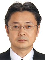 Ken Morito received the B.E., M.E., and Ph.D. from the Tokyo Institute of Technology. In 1990, he joined Fujitsu Laboratories Ltd. and has been engaged in the development of III-V based photonic devices; electro-absorption modulator integrated DFB lasers (EML), wavelength tunable lasers, semiconductor optical amplifiers (SOA), optical coupler integrated SOA gate array switches, 90degree hybrid and integrated optical receivers. From 1996 to 1997, he was a Visiting Researcher at the Swiss Federal Institute of Technology in Zurich (ETHZ), where he was engaged in the research on ultrafast all-optical switches. In 2012 he joined Photonics Electronics Technology Research Association (PETRA) and has developed Silicon photonics devices; III-V and Si hybrid lasers, optical Mux/DeMux filters and integrated optical transceivers. Dr. Morito is a member of the IEEE, the IEICE and the Japan Society of Applied Physics. He served on program committees of international conferences including OFC, OAA, OECC, LEOS, COIN and IPRM.
The definitions and distinctions between memory and storage have been clear for some time. However, a number of factors including the virtualized overhaul of the data center, the slowing of Moore’s law, and the slowing of DRAM scaling are going to blur the line between storage and memory. This talk will explain the convergence of technologies between storage system and memory systems that may result.
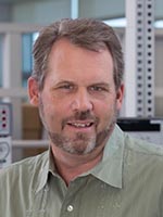 Craig Hampel has spent 30 years designing and developing leading edge memory systems. He has been involved in numerous proprietary and standards based memory initiatives and has developed a unique understanding of the technical and economic catalysts in the memory and storage industry. He has been awarded over 200 patents in memory and memory interfaces, has received numerous awards for innovation, and contributed to memory systems ranging from game consoles to supercomputers. Craig is currently involved in looking at the future of memory in systems with new computing models like quantum computing.
This talk will follow the data stream in 5G telecommunication systems from data center/service provider gateway to the core network and RAN connectivity through to the end user hardware. Relevant system architectures along the data path are detailed and the influence of key system performance metrics are related to semiconductor technology platform requirements. Technologies considered will include scaled digital CMOS, high performance RF (uW and mmWave), high speed interconnect (silicon photonics) and storage.
 Ted Letavic has a PhD in Electrical Engineering from Rensselaer Polytechnic Institute, and over 25 years of experience in the research, development, and industrialization of semiconductor systems. Ted has served on the Industrial Advisory Board to the US National Science Foundation, and serves on the executive committee for the IEEE/EDS International Symposium on Power Semiconductor Devices and ICs. He has 55 US patents granted, has authored over 70 reviewed scientific papers (10 invited/plenary), and has co-authored one textbook. Ted is a Senior Director, GLOBALFOUNDRIES, with responsibility for system architecture and semiconductor technology market requirements for strategic and emerging applications.
The exponential growth of information generated by humans and objects creates an explosion of digital data and the need for fast data analysis while keeping a constant energy envelope. This will cause a paradigm shift for computing infrastructures to move from a tight focus on performance towards energy-efficiency and total cost of ownership. The components of future servers and their integration into a full system must be reconsidered. This will be made possible with the emergence of new technologies and solutions to increase compute density and energy efficiency, to minimize the cost of data movement and to optimize the cost of new Integrated Circuit design and manufacturing.
3D System-on-Chip (SoC) and 2D heterogeneous system integration bring solutions for the challenges of i) density (with 3D memories and monolithic SoC), ii) energy efficiency and low power data movement (by reducing the length of interconnections), iii) specialization and cost (making a “System on Interposer” composed of functions), iv) heterogeneity (by manufacturing each component using the optimal technology level). This lecture will explore integration technologies from 2D heterogeneous to 3D SoC, from system architecture partitioning to integration technology for advanced computing. The lecture audience will receive a comprehensive overview of 3D and 2D integration technologies and their applications for Cloud Computing.
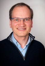 Denis Dutoit joined CEA-Leti in 2009, after working for STMicroelectronics and STEricsson where he has held several positions from digital circuit designer to digital SoC architecture manager. In CEA-Leti, he has been involved in System-on-a-Chip architecture for computing and 3D Integrated Circuit projects; he has been the lead architect of several designs all combining low power, 3D integration, many core architecture and Network-on-Chip. He is now strategic marketing manager in charge of defining the Leti’s roadmap of technologies and solutions for advanced computing. He also coordinates the ExaNoDe European collaborative project aiming at Exascale compute node. Dr. Dutoit holds an engineering degree from the École Nationale Supérieure d’Électronique et de Radioélectricité de Grenoble, and a Ph.D. in signal processing from the École Nationale Supérieure des Télécommunications de Paris. He is a co-recipient of the Jan Van Vessem Award for Outstanding European Paper at ISSCC 2005.
Compound semiconductors (and mainly at the moment SiC and GaN) power devices have practically shown a quantum leap in the performances of power devices and in the possibility to enlarge the use of power electronics especially at very high voltages and high power. However, the status of SiC and GaN devices today is much less mature than that of Si power devices in terms of manufacturability, material quality and process control, cost and reliability. In this talk activities on SiC and GaN power devices at STMicroelectronics will be presented.
SiC devices (Power Schottly, MOSFETs) in the fast few years has moved from academic curiosity and outstanding proof of concepts to products with excellent performances and proven reliability. Progress in the quality of substrates and epitaxial layers has been outstanding and evidences will be given on how the screening of residual defects is of paramount importance to achieve high yield and reliability. Also, performances of current products will be presented and roadmaps highlighted. GaN Devices are also getting out of simple academic curiosity and are promising not only to enlarge the field of use of power devices but also to challenges Si in some of today markets. It will be shown that performances of GaN HEMT devices and the possibility to build them on GaN epitaxial layers grown on Si are opening paths to this scenario. However, especially for high voltage devices (600 V and above), robustness in term of final reliability in the application has to be improved, in spite of the fact that significant progresses in understanding and correcting some of the issues have been made in the last period.
For both SiC and GaN devices the expected trends of the cost/performances ratio will be presented. A benchmark with existing solutions based on Si-based power devices will be done in details.
 Salvatore Coffa was born in Carlentini, near Siracusa, Italy, in 1962. He received a degree in physics in 1985 and a Ph.D. in physics in 1991 from the University of Catania (Italy). Over a period of more than 20 years in research activity, Coffa has achieved many important research results in various fields and gained key expertise in the area of technology transfer from basic research ideas to prototypes and applications. Since January 2006 he has held the position of R&D Manager of the Industrial and Power Group (IPG) of STMicroelectronics. With the responsibility for a group of 400 people, Coffa supervises development programs in the fields of power electronics, healthcare, opto-electronics, energy generation (fuel cells and solar cells), and electronics on plastic. He is also responsible for the IPG laboratories for optoelectronics, bioelectronics and electronics on plastic which have been set up in Catania.
Coffa holds several patents and has authored more than 200 publications in international journals. Internationally he is recognized as one the world leaders in the field of Si-based integrated photonics and as an outstanding material scientist. His group interacts with many other companies as well as academic and research institutions in Italy and abroad.
II. The Beyond: Edge Computing and Emerging Horizons
The proliferation of sensors into our daily environment or even on or into our human bodies raises the need for data analysis and information extraction at the source. Transmitting all the raw data is just inefficient, clogs the network, and poses security and privacy issues. In-sensor processing hence will become a necessity. To scale to the available energy sources and the sizes of the sensor nodes will require a further scaling of the computational energy with one or two orders of magnitude, especially if the type of processing required supersedes simple feature extraction or artifact removal. In this lecture, we will explore a number of ways on how the order of magnitude in energy reduction may be obtained.
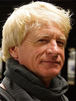 Jan Rabaey has made high-impact contributions to a number of fields, including advanced wireless systems, sensor networks, configurable ICs and low-power design. His current interests include the conception and implementation of next-generation integrated wireless systems over a very broad range of applications, as well as exploring the interaction between the cyber and the biological world. After receiving his Ph.D. degree in Applied Sciences from the Katholieke Universiteit Leuven, Belgium in 1983, he joined the University of California, Berkeley as a Visiting Research Engineer. From 1985 to1987 he was a research manager at IMEC, Belgium, and in 1987 he joined the faculty of the Electrical Engineering and Computer Science department of the University of California, Berkeley. From 1999 until 2002, he was the Associate Chair of the EECS department at UC Berkeley. He is the past director of the FCRP Gigascale Systems Research Center (GSRC) and the Multiscale Systems Center (MuSyC). He is an IEEE Fellow and member of the Royal Flemish Academy of Sciences and Arts, and recipient of the 2008 IEEE CAS Mac Van Valkenburg, the 2009 EDAA Lifetime Achievement, and the 2010 Semiconductor Industry Association University Researcher Awards. He has been involved in a broad range of startup companies.
Towards the Internet of Everything (IoE) era, it could be strongly required to make the power dissipation greatly low in VLSI computing, while still increasing high-performance computing power. However, in the present CMOS-only-based VLSI computing, there are some essential problems; communication bottleneck between memory and logic modules inside a VLSI chip, as well as increasing standby power dissipation and device-characteristic variation effect, which limits opening up the IoE era. In conventional logic-LSI architecture, logic and memory modules are separately implemented together and these modules are connected each other through global interconnections. Even if the device feature size is scaled down in accordance with the semiconductor technology roadmap, the global interconnections are not shorten, rather than are getting longer, which resulting in longer delay and higher power dissipation due to interconnections. In addition, since on-chip memory modules are “volatile,” they always consume the static power to maintain the stored data. In my talk, novel logic-LSI architecture, called “MOS/MTJ-hybrid integrated circuits with nonvolatile logic-in-memory (NV-LIM) architecture,” where nonvolatile MTJ (magnetic tunnel junction) elements are distributed over a logic-circuit plane, is introduced as a promising candidate to overcome performance wall and power wall due to the present CMOS-only-based logic-LSIs. Some concrete design examples based on the NV-LIM architecture are demonstrated and their usefulness is discussed in comparison with the corresponding CMOS-only-based.
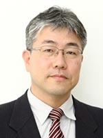 Takahiro Hanyu received the B.E., M.E. and D.E. degrees in Electronic Engineering from Tohoku University, Sendai, Japan, in 1984, 1986 and 1989, respectively. He is currently a Professor in the Research Institute of Electrical Communication, Tohoku University. His general research interests include nonvolatile logic circuits and their applications to ultra-low-power and/or highly dependable VLSI processors. He received the Sakai Memorial Award from the Information Processing Society of Japan in 2000, the Judge’s Special Award at the 9th LSI Design of the Year from the Semiconductor Industry News of Japan in 2002, the Special Feature Award at the University LSI Design Contest from ASP-DAC in 2007, the APEX Paper Award of Japan Society of Applied Physics in 2009, the Excellent Paper Award of IEICE, Japan, in 2010, Ichimura Academic Award in 2010, the Best Paper Award of IEEE ISVLSI 2010, the Paper Award of SSDM 2012, the Best Paper Finalist of IEEE ASYNC 2014, and the Commendation for Science and Technology by MEXT, Japan in 2015. Dr. Hanyu is a Senior Member of the IEEE.
For more than 50 years, the capabilities of Von Neumann-style information processing systems — in which a “memory” delivers operations and then operands to a dedicated “central processing unit” — have improved dramatically. While it may seem that this remarkable history was driven by ever-increasing density (Moore’s Law), the actual driver was Dennard’s Law: the amazing realization that each generation of scaled-down transistors could actually perform better, in every way, than the previous generation. Unfortunately, Dennard’s Law terminated some years ago, and as a result, Moore’s Law is now slowing considerably. In a search for ways to continue to improve computing systems, the attention of the IT industry has turned to Non-Von Neumann algorithms, and in particular, to computing architectures motivated by the human brain. In this talk, we will review recent progress towards hardware implementation and/or acceleration of such brain-inspired computing architectures. This progress ranges from systems that combine conventional CMOS devices in different and unconventional ways, to systems built around emerging NVM (Non-Volatile Memory) devices; and from systems designed to accelerate conventional ML (Machine Learning) through hardware innovation, to systems that seek to transcend the limitations of current ML algorithms, which tend to require large datasets of static, labeled data.
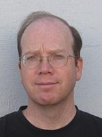 Geoffrey W. Burr received his Ph.D. in Electrical Engineering from the California Institute of Technology in 1996. Since that time, Dr. Burr has worked at IBM Almaden – Research in San Jose, California, where he is currently a Principal Research Staff Member. He has worked in a number of diverse areas, including holographic data storage, photon echoes, computational electromagnetics, nanophotonics, computational lithography, phase-change memory, storage class memory, and novel access devices based on Mixed-Ionic-Electronic-Conduction (MIEC) materials. Dr. Burr’s current research interests include non-volatile memory and cognitive (neuromorphic) computing. An IEEE Senior Member, Geoff is also a member of MRS, SPIE, OSA, Tau Beta Pi, Eta Kappa Nu, and the Institute of Physics (IOP).
Flexible and stretchable electronic devices are expected to open up a new class of applications ranging from flexible displays, wearable sensors, to flexible actuators. As one of the promising applications of flexible and stretchable electronics, biomedical sensors have attracted much attention recently. Sensors and electronic circuits for healthcare and medical applications have been fabricated using silicon and other rigid electronic materials. In order to minimize the discomfort of wearing rigid sensors, it is highly desirable to use soft electronic materials particularly for devices that come directly into contact with the skin and/or biological tissues. In this regard, electronics manufactured on thin polymeric films are very attractive. In this talk, we report on the recent progresses of thin, lightweight, flexible, and even stretchable devices and sensors especially for healthcare and biomedical applications.
 Takao Someya received the Ph.D. degree in electrical engineering from the University of Tokyo in 1997. Since 2009, he has been a professor of Department of Electrical and Electronic Engineering, The University of Tokyo. From 2001 to 2003, he worked at the Nanocenter (NSEC) of Columbia University and Bell Labs, Lucent Technologies, as a Visiting Scholar. His current research interests include organic transistors, flexible electronics, plastic integrated circuits, large-area sensors, and plastic actuators. Prof. Someya has received a number of awards, a Japan Society for the Promotion of Science (JSPS) Prize in 2009, 2004 IEEE/ISSCC Sugano Award, and 2009 IEEE Paul Rappaport Award. Prof. Someya’s “large-area sensor array” electronic thin film was featured in Time Magazine as one of its “Best Inventions of 2005” in its November 21st, 2005 issue.
Mobile Devices are an integral part of our modern lifestyle. Laptop PCs have evolved over the years into new and exciting form factors such as 2-in-1 detachables, 2-in-1 convertibles, and very thin and light designs, in many cases, offering desktop equivalent performance and longer battery life. Given our desire to be connected anywhere, anytime longer battery life continues to rank in top 3 user preferences. High performance, stunning visual displays, and thin designs make delivering longer battery life a significant challenge. This presentation will discuss motivation for longer battery life, factors contributing to mobile PC platform power consumption, technologies to lower SoC, display subsystem, and application power consumption. Finally, we will close the talk with an innovative solution that provides for a faster, cheaper, and accurate platform power measurement solution specifically targeted for software developers.
Kamal Shah is the director of system architecture in Intel’s client computing group where he is responsible for management of advanced platform architecture. He is also the chairman of Mobile PC Extended Battery Life Working Group, an industry group focused on the vision of all day and beyond of battery life of mobile PCs. He is routinely invited to speak at display, power sources, and power management conferences. He holds M.S. in Computer Engineering from University of Texas at Austin and is an author of two granted patents.
2016 Silicon Nanoelectronics Workshop will be co-located with the Symposia on Sunday and Monday, June 12-13, 2016 at the Hilton Hawaiian Village.
2016 Spintronics Workshop on LSI will be co-located with the Symposia at a date to be announced.