PLENARY & PANELS

Technology Plenary Session

Pandemic Challenges, Technology Answers

Dr. Siyoung Choi

President, General Manager of Foundry Business, Device Solutions Division, Samsung Electronics

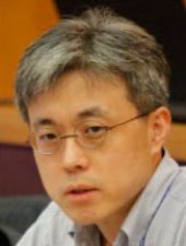
Dr. Siyoung Choi is the president and general manager of foundry business in Samsung Electronics' Device Solutions Division. Prior to his position, he was the head of Foundry and Memory Manufacturing Technology Center, respectively. His experience of Memory and Logic Process Development Team in Semiconductor R&D Center and of Manufacturing Technology Center brings his technology and operation leadership to foundry business unit. Since joining Samsung Electronics in 1995, Dr. Choi has played a pivotal role in developing advanced process technologies across memory and logic ICs that greatly strengthened Samsung's leading position in the semiconductor market. Under his leadership, Samsung successfully launched world’s first V-NAND and industry's first SoCs based on 14nm and 10nm FinFET process technologies. During his tenure as the head of manufacturing technology center, he successfully led establishing the world's largest semiconductor manufacturing cluster. Moreover, he spearheaded the innovation of manufacturing system to greatly strengthen fab operation efficiency as well as maximize technology competitiveness. Dr. Choi has been awarded the Gold Tower Order of Industrial Service Merit, the highest honor, by the Korean government for his contributions to the advancement of technology. He has written/co-authored over 110 technical publications and also holds over 100 U.S. patents. He also has been serving as a member of numeral technical committees including VLSI, ITRS, and IMEC. He holds B.S. and M.S. in Materials Science and Engineering from Yonsei University and a Ph.D in Materials Science and Engineering from Ohio State University.

Abstract:
As the global community was caught off guard with the pandemic, semiconductor industry dealt with unexpected swings in applications and demands. Health crisis created an immediate need for social distancing that disconnected and disrupted human interactions, and technology had to step up on short notice to mend and reconnect communities. In this paper, we share the insights we gained as the semiconductor technologists who were called to provide solutions in a nimble and yet comprehensive manner to deal with the unexpected, and offer our vision and new model for the foundries, not just as the manufacturers, but as solution providers. The new market reality dominated by “untact” and “connect” demand differentiated strategies in providing foundry solutions, which include close engagement with customers in earlier stages of technology R&D, as well as design infrastructure tailored to customers’ specific requirements. We present our vision to drive such change in foundry technology directions.

Materials to Systems in Semiconductor Manufacturing and Beyond

Dr. Om Nalamasu

Senior Vice President, Chief Technology Officer, Applied Materials, Inc.
President, Applied Ventures, LLC

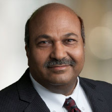
Dr. Omkaram (Om) Nalamasu is senior vice president and chief technology officer (CTO) of Applied Materials, Inc. He brings extensive experience and passion to the role of CTO, where he leads the development of disruptive products to address new markets and businesses in partnership with the broader technology ecosystem. He has built a world-class team to support Applied’s leadership in materials engineering. He also serves as president of Applied Ventures, LLC, the venture capital fund of Applied Materials, where he oversees strategic investments in early- and growth-stage companies. A world-renowned expert in materials science and one of our industry’s most respected forward-thinkers, Dr. Nalamasu has championed a renewed focus on Applied’s global innovation culture through various internal development programs and open innovation methods. He has solidified strategic relationships with universities, government organizations and research institutes around the world. Dr. Nalamasu joined Applied in 2006 after serving as an NYSTAR Distinguished Professor of materials science and engineering at Rensselaer Polytechnic Institute, where he also served as vice president of research. He has held key research and development leadership positions at AT&T Bell Laboratories, Bell Laboratories/Lucent Technologies, and Agere Systems, Inc., and was director of Bell Laboratories‘ Nanofabrication Research Laboratory, MEMS and Waveguides Research, and Condensed Matter Physics organizations. His research interests include nanomanufacturing, nanopatterning, electronic and photonic materials, and lithography, with special emphasis on applying patterning and materials expertise for device fabrication for electronics, photonics and energy applications. Dr. Nalamasu has made seminal contributions to the fields of optical lithography and polymeric materials science and technology. He has received numerous awards, authored more than 180 papers, review articles and books, and holds more than 120 worldwide issued patents. In 2017, Dr. Nalamasu was elected to the U.S. National Academy of Engineering for technical innovation spanning materials development, atomically controlled thin-film fabrication, and commercialization in microelectronics and energy generation and storage. He is a member of the board of directors of The Tech Museum in Silicon Valley and serves on several national and international advisory boards. He received his Ph.D. from the University of British Columbia, Vancouver, Canada.

Abstract:
Material engineering, the ability to manipulate materials with atomic control on an industrial scale has been the foundation for semiconductor technology innovations. Materials engineering combined with integrated processing, co-optimization, and artificial intelligence (AI) are the foundational elements of technology to advance semiconductor technology innovations and commercialization. Material engineering can provide solutions spanning materials creation, modification, removal and analysis. Integrated process and co-optimization can augment the power of unit process technology to unprecedented capability and significantly speed up process development and time to market. The advances of big data and AI can be leveraged to improve process margin, and repeatability, tool performance matching and uptime, and fabrication yield and variability. For VLSI semiconductor manufacturing, the materials-to-systems strategy would encompass integrated process solutions, advanced packaging, actionable insight accelerator and more than Moore to drive the PPACt (performance, power, area-cost and time-to-market) of VLSI ecosystem forward. Moreover, it can be used to enable other high-tech inflections such as life science, energy storage and generation, advanced imaging and future display.


Circuits Plenary Session

Fugaku and A64FX: The First Exascale
Supercomputer and its Innovative Arm CPU

Dr. Satoshi Matsuoka

Director, Center for Computational Science (R-CCS), Riken

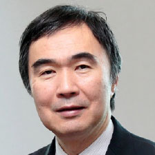
Satoshi Matsuoka from April 2018 has become the director of Riken CCS, the top-tier HPC center that represents HPC in Japan, developing and hosting Japan’s tier-one ‘Fugaku’ supercomputer which has become the fastest supercomputer in the world in all four major supercomputer rankings, along with multitudes of ongoing cutting edge HPC research being conducted, including investigating Post-Moore era computing. He had been a Full Professor at the Global Scientific Information and Computing Center (GSIC), the Tokyo Institute of Technology since 2000, and the director of the joint AIST Tokyo Tech. Real World Big Data Computing Open Innovation Laboratory (RWBCOIL) since 2017, and he became a Specially Appointed Professor at Tokyo Tech in 2018 along with his directorship at R-CCS. He has been the leader of the TSUBAME series of supercomputers that have won many accolades such as world #1 in power-efficient computing. He also leads various major supercomputing research projects in areas such as parallel algorithms and programming, resilience, green computing, and convergence of big data/AI with HPC. He has written over 500 articles according to Google Scholar, and chaired numerous ACM/IEEE conferences, including the Program Chair at the ACM/IEEE Supercomputing Conference (SC13) in 2013. He is a Fellow of the ACM and European ISC, and has won many awards, including the JSPS Prize from the Japan Society for Promotion of Science in 2006, presented by his Highness Prince Akishino; the ACM Gordon Bell Prize in 2011; the Commendation for Science and Technology by the Minister of Education, Culture, Sports, Science and Technology in 2012; the 2014 IEEE-CS Sidney Fernbach Memorial Award, the highest prestige in the field of HPC; HPDC 2018 Achievement Award from ACM; and recently SC Asia 2019 HPC Leadership Award.

Abstract:
Fugaku is the first exascale supercomputer in the world, designed and built primarily by Riken Center for Computational Science (R-CCS) and Fujitsu Ltd., but involving essentially all the major stakeholders in the Japanese HPC community. The name ‘Fugaku’ is an alternative name for Mt. Fuji, and was chosen to signify that the machine not only seeks very high performance, but also a broad base of users and applicability at the same time. The heart of Fugaku is the new Fujitsu A64FX Arm processor, which is 100% compliant to Aarch64 specifications, yet embodies technologies realized for the first time in a major server general-purpose CPU, such as 7nm process technology, on-package integrated HBM2 and terabyte-class SVE streaming capabilities, on-die embedded TOFU-D high-performance network including the network switch, and adoption of so-called ‘disaggregated architecture’ that allows separation and arbitrary combination of CPU core, memory, and network functions. Fugaku uses 158,974 A64FX CPUs in a single socket node configuration, making it the largest and fastest supercomputer ever created, signified by its groundbreaking achievements in major HPC benchmarks, as well as producing societal results in COVID-19 applications.


A New Era of Tailored Computing

Mr. Mark Papermaster

CTO and EVP, Technology and Engineering, Advanced Micro Devices, Inc.

Mark Papermaster is Chief Technology Officer and Executive Vice President of Technology and Engineering at AMD and is responsible for corporate technical direction, product development including system-on-chip (SOC) methodology, microprocessor design, I/O and memory and advanced research. He led the re-design of engineering processes at AMD and the development of the award-winning “Zen” high-performance x86 CPU family, high-performance GPUs and the company’s modular design approach, Infinity Fabric. He also oversees Information Technology that delivers AMD’s compute infrastructure and services. His more than 35 years of engineering experience includes significant leadership roles managing the development of a wide range of products, from microprocessors to mobile devices and high-performance servers. Before joining AMD in October 2011 as Chief Technology Officer and Senior Vice President, Papermaster was the leader of Cisco’s Silicon Engineering Group, the organization responsible for silicon strategy, architecture, and development for the company’s switching and routing businesses. He served as Apple Senior Vice President of Devices Hardware Engineering, where he was responsible for iPod and iPhone hardware development. He also held a number of senior leadership positions at IBM overseeing development of the company’s key microprocessor and server technologies. Papermaster received his bachelor’s degree from the University of Texas at Austin and master’s degree from the University of Vermont, both in Electrical Engineering. He is a long-term member of the University of Texas Cockrell School of Engineering Advisory Board, Olin College Presidents Council and the Juvenile Diabetes Research Foundation. Most recently, he was appointed to the CTO Forum Advisory Board and IEEE Industry Advisory Board.

Abstract:
The worldwide computing market grew tremendously over the past decades, and looking toward the future, these trends do not appear to be slowing down. Moore’s Law coupled with incredible innovation in hardware and software are engines driving this growth. However, the entire industry faces a barrage of challenges including the slowing of Moore’s Law, stringent power and energy constraints, an always-connected society, and disruptions from the on-going artificial intelligence revolution. To continue delivering ever higher-performance computing solutions amid these difficulties, the industry needs to pivot to a new mindset of “Tailored Computing.” The need for and opportunities to tailor our technologies in all aspects of future compute will propel the industry toward heterogeneity in everything it does.