PLENARY & PANELS

Plenary Session 1

Date & Time: 8:00A.M.-10:00A.M. on June 13 (Tue)

PL1-1

Multi-Chiplet Heterogeneous Integration Packaging for Semiconductor System Scaling.

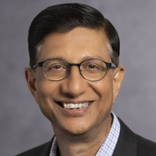
Dr. Surya Bhattacharya

Director, System-in-Package, Institute of Microelectronics, Agency for Science, Technology and Research (A*STAR)

Dr. Surya Bhattacharya is Director, System-in-Package, at A*STAR Institute of Microelectronics (IME), Singapore.  Over the past 30 years, he has worked on CMOS technology development, high volume product manufacturing, and advanced package scaling at integrated device manufacturer (IDM), fabless companies, and research institute.   At IME, Surya leads the packaging team to initiate and execute industry consortia projects to address challenges in advanced heterogeneous integration for system scaling.  Before joining IME, he served as Director of Foundry Engineering at Qualcomm, working on technology bring-up and product ramps at leading foundries.  Prior to Qualcomm, he was a Principal Foundry Engineer at Broadcom.  He started his career at Rockwell Semiconductor Systems, where he was Senior Manager for CMOS technology development.  Surya has a PhD in Electrical Engineering from the University of Texas at Austin, and B.Tech in Electrical Engineering from the Indian Institute of Technology, Madras.

Abstract:
Since the invention of the transistor, we have enjoyed tremendous impact of semiconductors on electronic systems. Transistor scaling has played a critical role in achieving increased functionality of semiconductor systems in main-frames, personal computers, and mobile phones by enabling lower power, cost and area per function through monolithic System-on-Chip (SoC). However, over the past decade, the diverse system requirements from wide ranging markets have driven the industry to use heterogeneous integration of multiple chiplets enabled by advanced packaging as a key new toolbox for System-in-Package scaling. This paper provides an overview of multi-chiplet heterogeneous integration (MCHI) packaging platforms to address system scaling needs in coming decades.

PL1-2

A Six-Word Story on the Future of VLSI:AI-driven, Software-defined, and Uncomfortably Exciting

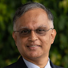
Dr. Parthasarathy Ranganathan

VP, Technical Fellow, Google LLC

Parthasarathy (Partha) Ranganathan is currently a VP, technical Fellow at Google where he is the area technical lead for hardware and datacenters, designing systems at scale. Prior to this, he was a HP Fellow and Chief Technologist at Hewlett Packard Labs where he led their research on systems and data centers.  Partha has worked on several interdisciplinary systems projects with broad impact on both academia and industry, including widely-used innovations in energy-aware user interfaces, heterogeneous multi-cores, power-efficient servers, accelerators, and disaggregated and data-centric data centers. He has published extensively (including being the co-author on the popular "Datacenter as a Computer" textbook), is a co-inventor on more than 100 patents, and has been recognized with numerous awards. He has been named a top-15 enterprise technology rock star by Business Insider, one of the top 35 young innovators in the world by MIT Tech Review, and is a recipient of the ACM SIGARCH Maurice Wilkes award, Rice University's Outstanding Young Engineering Alumni award, and the IIT Madras distinguished alumni award. He is also a Fellow of the IEEE and ACM, and is currently on the board of directors for OpenCompute.

Abstract:
We are at an interesting inflection point in the design of computing systems. On one hand, demand for computing is accelerating at phenomenal rates, powered by the AI revolution and ever deeper processing on larger volumes of data, and amplified by smart edge devices and cloud computing. On the other hand, Moore’s law is slowing down. This is challenging traditional assumptions around cheaper and more energy-efficient systems every generation, and leading to a significant supply-demand gap for future computing systems. In this paper, we discuss how this current computing landscape motivates a significant rethinking of how we design future hardware. We present two broad themes around (1) efficient design of hardware through custom silicon accelerators and (2) efficient utilization of hardware through software-defined systems design. Summarizing our experience in these areas, we identify key learnings and future opportunities for innovation. Looking ahead, we discuss some additional grand challenges and opportunities for the community, specifically touching on key themes around agility, modularity, reliability, and sustainability, as well as the disruptive potential of using machine learning for hardware design, and the opportunities beyond compute, around storage.


Plenary Session 2

Date & Time: 8:00A.M.-10:00A.M. on June 14 (Wed)

PL2-1

Quantum Computing from Hype to Game Changer

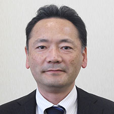
Dr. Hiroyuki Mizuno

Distinguished Researcher, Hitachi Ltd.

Hiroyuki Mizuno received the M.S., and Dr.Eng. degrees in electronic engineering from Osaka University, Osaka, Japan, in 1993 and 2001. In 1993 he joined Hitachi, Ltd., Tokyo, Japan where he designed high-speed and low-power circuits for SRAMs, microprocessors (SuperH), system-on-a-chip (SH-Mobile). From 2002 to 2003, he was a visiting scholar at the Department of Computer Science, Stanford University, Stanford, CA. He is a pioneer in quantum-inspired computing and presented CMOS annealing in 2015. He is the project manager of the Large-Scale Silicon Quantum Computing Project, one of the Moonshot R&D programs launched by the Cabinet Office starting in 2020. He is currently a distinguished researcher at Hitachi, and the laboratory manager of the Hitachi-Kyoto University Laboratory. At Hitachi-Kyoto University Laboratory, he researches Cyber Human Social Systems (CHSS) and Emotional Intelligence (EI), where humanities and social sciences, brain science (neuroscience), and artificial intelligence (AI) are deeply intersected. He has served in various roles for international conferences, including the technical program committees of the ISSCC from 2004 to 2007. He is a Fellow of the IEEE and a member of the ACM.

Abstract:
This paper describes the current state of quantum computer development in the world (including the hype) from three perspectives and introduces our research and development of quantum computers. The first is the complex market structure. While investments in quantum computers are increasing, these investments do not always immediately bring value to consumers, and this delay results in hype. CMOS annealing technology to fill this delay is described. The second is the accountability of the impact produced by a quantum computer that does not yet exist. This paper discusses why so many people continue to question the value of quantum computers despite their clear applications, and our struggles. The third is technology development, which includes many research aspects. This paper introduces our top-down approach that takes full advantage of semiconductor technologies. Some of our activities including “Shuttling qubit” for the next milestone in the development of silicon quantum computers, which is qubit operation in a scalable qubit array structure, are also described.


PL2-2

Searching for Nonlinearity: Scaling Limits in NAND Flash

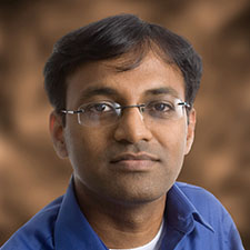
Dr. Siva Sivaram

President, Western Digital Corporation

Dr. Siva Sivaram is the President of Western Digital Corporation. He leads corporate strategy and development of silicon technologies and their high-volume manufacturing across sites around the globe.
Dr. Sivaram has over 30 years of experience in semiconductors, 3D memory architectures, process technology and equipment and materials. He has held executive positions at Intel and Matrix Semiconductor, and at SanDisk after its acquisition of Matrix. Additionally, he was the Founder and CEO of Twin Creeks Technologies, a solar panel and equipment company.
Dr. Sivaram is widely published, with works including a textbook on Chemical Vapor Deposition and he holds several patents in semiconductor and solar technologies. He serves on the executive board of the Silicon Valley Leadership Group, the board of the Global Semiconductor Association, and is the Vice Chairman of US India Business Council. He is the Chairman of Akshaya Patra, USA, the world’s largest NGO feeding school children.
Dr. Sivaram earned his doctorate and master’s degrees in Material Science from Rensselaer Polytechnic Institute, where he has been elected to its Board of Trustees. He is a Distinguished Alumnus of the National Institute of Technology, Trichy, India, where he earned his Bachelor’s Degree in Mechanical Engineering.

Abstract:
Data generation is growing at an exponential rate and the market opportunity for data storage is vast. However, there is still a substantial difference in the amount of data created versus data stored, driven by price elasticity of demand in the storage media. Pricing lies in the balance of supply and demand, but for NAND manufacturers to be profitable, cost is the driver for consistent price decline and will ultimately determine the amount of data stored. In this talk, we show that as NAND Flash moves into a mature era of 3D scaling using only increasing layer count results in a sub-linear cost reduction while producing higher bit growth. This breaks the virtuous cycle of growth, producing more bits than the market can absorb at a given price point and challenges the affordability of future investments. NAND scaling needs to move away from solely increasing layer count and instead seeking new avenues for reducing cost and complexity. Equipment productivity and reduction in consumables remain critical focus areas for the supply chain to contribute to cost reduction. Wafer bonding technology can be an enabler for new opportunities. It allows for decoupling the memory array from complex logic circuits, allowing new high speed logic integration with the memory layers, and simplifying manufacturing cycle times. This technology also allows the industry to move away from a one-size-fits-all NAND die to customized solutions for various applications and system level savings. Despite such breakthroughs, ultimately the health of the storage industry will be determined by fair distribution of the profit pool across the value chain commensurate with the R&D and capital spending by the different players.