Welcome to the 2011 Symposium on VLSI Technology
 PDF of Advance Program (as of May 18) PDF of Advance Program (as of May 18)
Program Changes (as of June 8)
PDF of Abstracts
Technical program at a glance
On behalf of the Organizing Committee, it is our great pleasure to invite you to the 2011 Symposium on VLSI Technology, which will be held from June 13-16 in Kyoto, Japan. This symposium has been recognized as one of the premiere technical conferences on the latest research and developments in the field of VLSI technologies and their applications, and this year is no exception even in the events of earthquakes and nuclear power plant, severely-influencing the northeastern part of Japan ONLY.
The Program Committee of this year has selected from 185 submitted papers 76 top quality papers addressing a wide range of topics, and 1 more outstanding quality paper has been adopted from 10 submitted papers as a Late News Paper. Furthermore, 12 speakers have been invited resulting in a total of 21 technical sessions organized this year.
We are also delighted to have two very distinguished invited speakers for the plenary session. M.D. and Ph.D. Makoto Nakamura, Professor at University of Toyama, will present a talk on “Computer-Assisted Biofabrication: The challenges on manufacturing 3-D biological tissues for tissue and organ engineering’’, and Dr. Samuel Naffziger, Corporate Fellow at AMD, will give a talk on “Technology Impacts from the New Wave of Architectures for Media-rich Workloads”.
Furthermore, we introduce two Focus Sessions, which cover the increasingly important fields of “Design Enablement including Manufacturing, Robustness and Innovation” and “3D LSI”. The design enablement session consists of 5 excellent invited speakers, in particular Professor Larry Pileggi of Carnegie Mellon University, Dr. Tomoaki Yabe of Toshiba, Dr. Andrew Brotman of Globalfoundries, Dr. Yohan Frans of Rambus, and Dr. Greg Northrop of IBM. Also the 3D LSI session corresponds to 5 excellent invited speakers, who are Dr. Jungdal Choi of Samsung, Dr. Pascal Ancey of STMicroelectronics, Dr. Giovanni De Michelis of EPFL, Dr. J. Bea of Tohoku University, and Dr. Jeffrey Burns of IBM TJ Watson Center.
Three Rump Sessions are planned in the evening of June 14 as a means to facilitate informal discussion among attendees. Two Technology Rump Sessions are regular sessions covering specific technologies related topics and are of timely interests
- “Can Fin-FET/FDSOI compensate for the stagnation in scaling?” as Technology Rump Session
- “Will emerging non-volatile memories finally emerge?” as Technology Rump Session
- “Low Voltage - How low can we go with Technology and Design Solutions?” for Joint Rump Session
A one-day Short Course scheduled for June 13 will address key challenges in the arena of CMOS logic and memory technologies and design enablement for future nodes and demonstrates that technology and circuit design co-optimization is required for further scaling: “Logic & Memory towards 15 nm node - Technology and Circuit Design Co-optimization “This should be an excellent opportunity for experienced as well as new engineers, for technologists as well as circuit designers, to broaden their technical base.
The symposium registration fee covers all of the sessions including the Rump Sessions, the symposium proceedings, the symposium banquet, and a CD-ROM containing all the contents of the Digests. A registration for the Short Course includes the attendance to the short course as well as a booklet containing the short course presentation materials. The detailed registration fees and hotel reservation schedules are included in the Web Advance Program.
We look forward to seeing you at this very exciting symposium in beautiful Kyoto, and we are sure that you will find the conference exciting and rewarding. |

Hitoshi Wakabayashi |
Klaus Schruefer |
| Program Chair |
Program Co-Chair |
CONFERENCE SCHEDULE
PROGRAM
Session 1 |
Welcome and Plenary Session [Shunju I, II] |
| Chairpersons |
H. Wakabayashi, Sony Corp.
K. Schruefer, Intel Mobile Communications GmbH |
8:30 |
1-1 |
Welcome and Opening Remarks |
| |
M. Niwa, Univ. of Tsukuba
M.-R. Lin, GLOBALFOUNDRIES |
8:45 |
1-2 |
Computer-Assisted Biofabrication: The Challenges on Manufacturing 3-D Biological Tissues for Tissue and Organ Engineering |
Invited
abstract |
M. Nakamura, S. Iwanaga, K. Arai, H. Tada, G. Capi and T. Nikaido, University of Toyama, Japan |
9:25 |
1-3 |
Technology Impacts from the New Wave of Architectures for Media-Rich Workloads |
Invited
abstract |
S. Naffziger, Adcanced Micro Devices, Inc., USA |
Session 2A |
FinFETs [Shunju I] |
| Chairpersons |
M. Masahara, AIST
T.-J. K. Liu, Univ. of California, Berkely |
10:40 |
2A-1 |
Scaling of SOI FinFETs Down to Fin Width of 4 nm for
the 10nm Technology Node |
| abstract |
J.B. Chang, M. Guillorn, P.M. Solomon, C.-H. Lin, S.U. Engelmann, A. Pyzyna, J.A. Ott and W.E. Haensch |
| IBM T.J. Watson Research Center, USA |
11:05 |
2A-2 |
Sub-25nm FinFET with Advanced Fin Formation and
Short Channel Effect Engineering |
| abstract |
T. Yamashita*, V.S.
Basker*, T. Standaert*, C.-C. Yeh*, T. Yamamoto***, K.
Maitra**, C.-H. Lin****, J. Faltermeier*, S. Kanakasabapathy*,
M. Wang*, H. Sunamura***, H. Jagannathan*, A. Reznicek*, S.
Schmitz*, A. Inada***, J. Wang*, H. Adhikari**, N. Berliner*, K-
L. Lee****, P. Kulkarni*, Y. Zhu****, A. Kumar****, A.
Bryant*, S. Wu*, T. Kanarsky*, J. Cho**, E. Mclellan*, S.J.
Holmes*, R.C. Johnson*, T. Levin*, J. Demarest*, J. Li*, P.
Oldiges*, J. Arnold*, M. Colburn*, M. Hane***, D. Mcherron*,
V.K. Paruchuri*, B. Doris*, R.J. Miller**, H. Bu*, M. Khare*, J.
ONeill* and E. Leobandung* |
| *IBM Research,
**GLOBALFOUNDRIES Inc., ***Renesas Electronics Corp. and
****IBM T.J. Watson Research Center, USA |
11:30 |
2A-3 |
Modeling of Width-Quantization-Induced Variations in
Logic FinFETs for 22nm and Beyond |
| abstract |
C.-H. Lin*, W.
Haensch*, P. Oldiges**, H. Wang**, R. Williams**, J. Chang*,
M. Guillorn*, A. Bryant*, T. Yamashita***, T. Standaert***, H.
Bu***, E. Leobandung* and M. Khare*** |
| *IBM T.J. Watson Research
Center, **IBM Systems and Technology Group and ***IBM
Research at Albany Nanotech, USA |
11:55 |
2A-4 |
Critical Discussion on (100) and (110) Orientation
Dependent Transport: nMOS Planar and FinFET |
| abstract |
C.D.
Young*, M.O. Baykan*,**, A. Agrawal***, H. Madan*,***, K.
Akarvardar*,****, C. Hobbs*, I. Ok*, W. Taylor*, C.E. Smith*,
M.M. Hussain*, T. Nishida**, S. Thompson**, P. Majhi*, P.
Kirsch*, S. Datta*** and R. Jammy*
|
| *SEMATECH, **U.
Florida-Gainesville, ***Penn State and ****GlobalFoundries
assignee, USA |
Session 2B |
RRAM I [Shunju II] |
| Chairpersons |
Y. Akasaka, TOKYO ELECTRON TAIWAN LIMITED
J. Zahurak, Micron Technology, Inc. |
10:40 |
2B-1 |
Forming-Free Nitrogen-Doped AlOx RRAM with Sub-µA
Programming Current |
| abstract |
W. Kim, S.I. Park, Z. Zhang, Y. Yang-Liauw, D. Sekar, H.-S. P. Wong and S.S. Wong |
| Stanford
University, USA |
11:05 |
2B-2 |
Evidences of Anodic-Oxidation Reset Mechanism in
TiN/NiO/Ni RRAM Cells |
| abstract |
L. Goux*, R. Degraeve*, B.
Govoreanu*, H.-Y. Chou**, V.V. Afanasev**, J. Meersschaut*,
M. Toeller***, X.P. Wang*, S. Kubicek*, O. Richard*, J.A.
Kittl*, D.J. Wouters*,**, M. Jurczak* and L. Altimime* |
| *IMEC,
**University of
Leuven, Belgium and ***Tokyo Electron Limited, Japan |
11:30 |
2B-3 |
Resistive Switching AlOx-Based Memory with CNT
Electrode for Ultra-Low Switching Current and High
Density Memory Application |
| abstract |
Y. Wu*, Y. Chai*,**, H.-Y.
Chen*, S. Yu* and H.-S. P. Wong* |
| *Stanford University, USA
and **Hong Kong University of Science and Technology, China |
11:55 |
2B-4 |
Deterministic and Stochastic Component in RESET
Transient of HfSiO/FUSI Gate RRAM Stack |
| abstract |
R. Degraeve*, L. Goux*, Ph. Roussel*, D.J. Wouters**, J.A. Kittl*, L. Altimime*, M. Jurczak*, G. Groeseneken** |
| *IMEC and **KU Leuven, Belgium |
Session 3A |
Advanced CMOS [Shunju I] |
| Chairpersons |
T. Hiramoto, The Univ. of Tokyo
T. Skotnicki, STMicroelectronics |
13:40 |
3A-1 |
Aggressively Scaled High-k Last Metal Gate Stack with
Low Variability for 20nm Logic High Performance and
Low Power Applications |
| abstract |
S. Hyun, J.-H. Han, H.-B. Park, H.-J.
Na, H.J. Son, H.Y. Lee, H.-S. Hong, H.-L. Lee, J. Song, J.J. Kim, J.
Lee, W.C. Jeong, H.J. Cho, K.I. Seo, D.W. Kim, S.P. Sim, S.B.
Kang, D.K. Sohn, S. Choi, H. Kang and C. Chung |
| Samsung
Electronics Co., Ltd., Korea |
14:05 |
3A-2 |
Gate-Last vs. Gate-First Technology for Aggressively
Scaled EOT Logic/RF CMOS |
| abstract |
A. Veloso*, L.-Å. Ragnarsson*,
M.J. Cho*, K. Devriendt*, K. Kellens*, F. Sebaai*, S. Suhard*, S.
Brus*, Y. Crabbe*, T. Schram*, E. Röhr*, V. Paraschiv*, G.
Eneman**, T. Kauerauf*, M. Dehan*, S.-H. Hong***, S.
Yamaguchi****, S. Takeoka*****, Y. Higuchi*****, H. Tielens*,
A. Van Ammel*, P. Favia*, H. Bender*, A. Franquet*, T.
Conard*, X. Li******, K.-L. Pey*******, H. Struyf*, P.
Mertens*, P.P. Absil*, N. Horiguchi* and T. Hoffmann* |
| *IMEC,
**also KU Leuven and FWO, assignees at IMEC from,
***Samsung, ****SONY, *****Panasonic, Belgium, ******IME,
A*STAR and *******SUTD, Singapore |
14:30 |
3A-3 |
Full Metal Gate with Borderless Contact for 14 nm and
Beyond |
| abstract |
S.-C. Seo*, L.F. Edge*, S. Kanakasabapathy*, M.
Frank****, A. Inada**, L. Adam*, M.M. Wang*, K. Watanabe**,
P. Jamison*, K. Ariyoshi***, M. Sankarapandian*, S. Fan*, D.
Horak*, J.T. Li*, T. Vo*, B. Haran*, J. Bruley****, M.
Hopstaken****, S.L. Brown****, J. Chang****, E.A. Cartier****,
D.-G. Park****, J.H. Stathis****, B. Doris*, R. Divakaruni*****,
M. Khare*, V. Narayanan**** and V.K. Paruchuri* |
| *IBM
Research, **Renesas Electronics Corp., ***Toshiba Corp. at Albany NanoTech, ****IBM
T.J. Watson Research Center and *****IBM Microelectronics,
USA |
14:55 |
3A-4 |
A 28nm Poly/SiON CMOS Technology for Low-Power
SoC Applications |
| abstract |
C.W. Liang, M.T. Chen, J.S. Jenq, W.Y.
Lien, C.C. Huang, Y.S. Lin, B.J. Tzau, W.J. Wu, Z.H. Fu, I.C.
Wang, P.Y. Chou, C.S. Fu, C.Y. Tzeng, K.L. Chiu, L.S. Huang,
J.W. You, J.G. Hung, Z.M. Cheng, B.C. Hsu, H.Y. Wang, Y.H. Ye,
J.Y. Wu, C.L. Yang, C.C. Huang, C.C. Chien, Y.R. Wang, C.C.
Liu, S.F. Tzou, Y.H. Huang, C.C. Yu, J.H. Liao, C.L. Lin, D.F.
Chen, S.C. Chien and I.C. Chen |
| United Microelectronics
Corporation Ltd. (UMC), Taiwan |
15:20 |
3A-5 |
RF and Mixed-Signal Performances of a Low Cost 28nm
Low-Power CMOS Technology for Wireless System-on-
Chip Applications |
| abstract |
M.-T. Yang, K. Liao, R. Welstand, C. Teng,
W. Sy, Y. Chen, R. Dutta, PR. Chidambaram, M. Han, Y. Du and
G. Yeap |
| Qualcomm Inc, USA |
Session 3B |
RRAM II [Shunju II] |
| Chairpersons |
S. S. Chung, National Chiao Tung Univ.
M. Khare, IBM Corp. |
13:40 |
3B-1 |
High Performance Unipolar AlOy/HfOx/Ni Based RRAM
Compatible with Si Diodes for 3D Application |
| abstract |
X.A. Tran*,
B. Gao*,**, J.F. Kang**, L. Wu*, Z.R. Wang*, Z. Fang*,***, K.L.
Pey*, Y.C. Yeo****, A.Y. Du*****, B.Y. Nguyen******, M.F.
Li******* and H.Y. Yu* |
| *Nanyang Technological University,
Singapore, **Peking University, China, ***A*STAR,
****National University of Singapore, *****GLOBALFOUNDRIES
Singapore, Singapore, ******Soitec, France and *******Fudan
University, China |
14:05 |
3B-2 |
Theoretical Study of the Resistance Switching
Mechanism in Rutile TiO2-x for ReRAM: the Role of
Oxygen Vacancies and Hydrogen Impurities |
| abstract |
S.G. Park, B.
Magyari-Köpe and Y. Nishi |
| Stanford University, USA |
14:30 |
3B-3 |
Highly Reliable and Fast Nonvolatile Hybrid Switching
ReRAM Memory Using Thin Al2 O3 Demonstrated at 54nm
Memory Array |
| abstract |
J. Yi, H. Choi, S. Lee, J. Lee, D. Son, S. Lee, S.
Hwang, S. Song, J. Park, S. Kim, W. Kim, J.-Y. Kim, S. Lee, J.
Moon, J. You, M. Joo, J. Roh, S. Park, S.-W. Chung, J. Lee and S.-
J. Hong |
| Hynix Semiconductor Inc., Korea |
14:55 |
3B-4 |
High Thermal Robust ReRAM with a New Method for
Suppressing Read Disturb |
| abstract |
M. Terai, M. Saitoh, T. Nagumo,
Y. Sakotsubo, Y. Yabe, K. Takeda and T. Hase |
| Renesas
Electronics Corp., Japan |
15:20 |
3B-5 |
Bi-Layered RRAM with Unlimited Endurance and
Extremely Uniform Switching |
| abstract |
Y.-B. Kim, S.R. Lee, D. Lee,
C.B. Lee, M. Chang, J.H. Hur, M.-J. Lee, G.-S. Park, C.J. Kim, U.-
I. Chung, I.-K. Yoo and K. Kim |
| Samsung Advanced Institute of
Technology, Korea |
Session 4A |
High Mobility Channel Devices [Shunju I] |
| Chairpersons |
C. H. Wann, TSMC
J. Kavalieros, Intel Corp. |
16:00 |
4A-1 |
High Mobility Ge pMOSFETs with ~ 1nm Thin EOT Using
Al2O3/GeOx/Ge Gate Stacks Fabricated by Plasma Post
Oxidation |
| abstract |
R. Zhang, T. Iwasaki, N. Taoka, M. Takenaka and S.
Takagi |
| The University of Tokyo, Japan |
16:25 |
4A-2 |
High Performance Extremely-Thin Body III-V-On-
Insulator MOSFETs on a Si Substrate with Ni-InGaAs
Metal S/D and MOS Interface Buffer Engineering |
| abstract |
S.H.
Kim*, M. Yokoyama*, N. Taoka*, R. Iida*, S. Lee*, R. Nakane*,
Y. Urabe**, N. Miyata**, T. Yasuda**, H. Yamada***, N.
Fukuhara***, M. Hata***, M. Takenaka* and S. Takagi* |
| *The
University of Tokyo, **National Institute of Advanced Industrial
Science and Technology and ***Sumitomo Chemical Co. Ltd.,
Japan |
16:50 |
4A-3 |
CMOS Integration of InGaAs
nMOSFETs and Ge
pMOSFETs with Self-Align Ni-Based Metal S/D Using
Direct Wafer Bonding |
| abstract |
M. Yokoyama*, S.H. Kim*, R. Zhang*,
N. Taoka*, Y. Urabe**, T. Maeda**, H. Takagi**, T. Yasuda**,
H. Yamada***, O. Ichikawa***, N. Fukuhara***, M. Hata***, M.
Sugiyama*, Y. Nakano*, M. Takenaka* and S. Takagi* |
| *The
University of Tokyo, **National Institute of Advanced Industrial
Science and Technology(AIST) and ***Sumitomo Chemical Co. Ltd.,
Japan |
17:15 |
4A-4 |
Scalable TaN Metal Source/Drain & Gate InGaAs/Ge
n/pMOSFETs |
| abstract |
T. Maeda*, Y. Urabe*, T. Itatani*, H. Ishii*, N.
Miyata*, T. Yasuda*, H. Yamada**, M. Hata**, M.
Yokoyama***, M. Takenaka*** and S. Takagi*** |
| *National
Institute of Advanced Industrial Science and Technology (AIST),
**Sumitomo Chemical Co. Ltd. and ***The University of Tokyo,
Japan |
17:40 |
4A-5 |
A 0.021 μm2 Trigate SRAM Cell with Aggressively Scaled Gate and Contact Pitch |
Late News
abstract |
M.A. Guillorn, J. Chang, A. Pyzyna, S. Engelmann, M. Glodde, E. Joseph, R. Bruce, J.A. Ott, A. Majumdar, F. Liu, M. Brink, S. Bangsaruntip, M. Khater, S. Mauer, I. Lauer, C. Lavoie, Z. Zhang, J. Newbury, E. Kratschmer, D.P. Klaus, J. Bucchignano, B. To, W. Graham, E. Sikorski, V. Narayanan, N. Fuller and W. Haensch |
| IBM T.J. Watson Research Center, USA |
Session 4B |
NAND Flash Memory [Shunju II] |
| Chairpersons |
S. Hong, Hynix Semiconductor Inc.
J. Zahurak, Micron Technology, Inc. |
16:00 |
4B-1 |
A Highly Scalable Vertical Gate (VG) 3D NAND Flash with
Robust Program Disturb Immunity Using a Novel PN
Diode Decoding Structure |
| abstract |
C.-H. Hung, H.-T. Lue, K.-P.
Chang, C.-P. Chen, Y.-H. Hsiao, S.-H. Chen, Y.-H. Shih, K.-Y.
Hsieh, M. Yang, J. Lee, S.-Y. Wang, T. Yang, K.-C. Chen and C.-
Y. Lu |
| Macronix International Co., Ltd., Taiwan |
16:25 |
4B-2 |
A Highly Manufacturable Integration Technology of 20nm
Generation 64Gb Multi-Level NAND Flash Memory |
| abstract |
K. W.
Lee, S.K. Choi, S.J. Chung, H.L. Lee, S.M. Yi, B.I. Han, B.I. Lee,
D.H. Lee, J.H. Seo, N.Y. Park, H.S. Kim, H.S. Kim, T.U. Youn,
K.H. Noh, M.K. Lee, J.Y. Lee, K.H. Han, W.S. Woo, S.W. Cho,
S.C. Lee, S.S. Kim, C.S. Hyun, W.J. Suh, S.D. Kim, M.K. Ahn,
H.S. Kim, K.S. Kim, G.S. Cho, S. K. Park, S. Aritome, J.W. Kim,
S.K. Lee, S.J. Hong and S.W. Park |
| Hynix Semiconductor Inc.,
Korea |
16:50 |
4B-3 |
A Novel Low-Voltage Hot-Carrier (LVHC) Programming
Method for Scaled NAND Flash Cell |
| abstract |
W.-J. Tsai, P.H. Tsai,
J.S. Huang, S.G. Yan, C.H. Cheng, C.C. Cheng, Y.J. Chen, C.H.
Lee, M.C. Hsu, T.T. Han, T.C. Lu, K.C. Chen and C.-Y. Lu |
| Macronix International Co., Ltd., Taiwan |
17:15 |
4B-4 |
A Novel Junctionless All-Around-Gate SONOS Device
with a Quantum Nanowire on a Bulk Substrate for 3D
Stack NAND Flash Memory |
| abstract |
S.-J. Choi, D.-I. Moon, J.P.
Duarte, S. Kim and Y.-K. Choi |
| KAIST, Korea |
17:40 |
4B-5 |
Extraction of 3-D Trap Position in NAND Flash Memory
Considering Channel Resistance of Pass Cells and Bit-
Line Interference |
Late News
abstract |
S.M. Joe*, M.K. Jung*, J.W. Lee*, M.S.
Lee*, B.S. Jo*, J.H. Bae*, S.K. Park**, K.R. Han**, J.H. Yi**,
G.S. Cho** and J.H. Lee* |
| *Seoul National University and
**Hynix Semiconductor Inc., Korea |
Tuesday, June 14
20:00-22:00 |
Rump Sessions
|
| Organizers |
N. Kasai, Tohoku Univ.
T. Skotnicki, STMicroelectronics |
J-R |
Low Voltage - How Low Can We Go with Technology and Design Solutions? [Suzaku I, II] |
| Organizers |
| Technology: |
N. Kasai, Tohoku Univ
T. Skotnicki, STMicroelectronics |
| Circutis: |
S. Dosho, Panasonic Corp.
M. Clinton, Texas Instruments, Inc. |
|
Moderators |
K. Ishimaru, Toshiba Corp.
K. Zhang, Intel Corp. |
Panelists |
F. Boeuf, STMicroelectronics
B. Calhoun, University of Virginia
M. Ieong, TSMC
K. Rim, IBM Corp.
S. Kosonocky, AMD
A. Matsuzawa, Tokyo Institute of Technology
S. Paak, Samsung Electronics
H. Shinohara, STARC |
Continually lowering IC voltage levels has been critical to continued device scaling for a long time, but now many circuit designers are finding it increasingly difficult to design robust circuits with the lower voltage levels. Is it possible that Moore’s Law will end due to our inability to reduce voltage levels, and not because of our inability to further scale transistors? We have assembled a distinguished panel to debate some of the following questions, and much more:
- What role does technology play in requiring lower operating voltages? What is the role of circuit design?
- Lower operating voltages cause problems (and benefits) for circuit designers, are there technology solutions to some of these problems? Conversely, if voltage levels are not scaled this will cause device problems and is it possible that there are circuit solutions to these technology problems?
- Are voltage levels low enough today, or how much lower can we expect them to go in the future?
|
R-1 |
Can FinFET/FDSOI Compensate for the Stagnation in Scaling? [Shunju I] |
| Organizers |
N. Kasai,Tohoku Univ.
T. Skotnicki, STMicroelectronics |
Moderators |
M. Hane, Renesas Electronics Corp.
C. Mazure, Soitec Group |
Panelists |
A. Strojwas, PDF Solution
C. Hu, University of California, Berkeley
K. Okada, Tokyo Institute of Technology
M. Bohr, Intel Corp.
M. Haond, STMicroelectronics
S. Venkatesan, GLOBALFOUNDRIES |
CMOS Bulk technology is facing serious issues with respect to further device down scaling in spite of the fact that many new technologies have successfully been developed, such as strain techniques, high-K dielectric and metal-gate-electrode. Despite that, performance scaling trend seems to stagnate when moving towards further advanced CMOS nodes. Fully-depleted (FD)-devices (planar SOI or Fin-type) are known as promising device structures for revitalizing CMOS scaling by means of the short-channel-effect mitigation, lower leakage, smaller variability, and so on. Such the new device structures will strongly impact not only on LSI core device/process technology but also on chip modules architecture and circuit design paradigm. This panel discussion will be aimed at addressing key challenges for the introduction of planar-FDSOI or Fin-FET in conjunction with future technology scaling prospects, and several key questions:
- How Fin-FET/FDSOI can be integrated within an LSI chip?
- On such a chip, should Fin-FET/FDSOI be applied for the whole area, including analog circuit, or for a partial area, such as SRAM blocks?
- Which generation would be practically viable for Fin-FET/FDSOI introduction and what are the specific reasons for this?
|
R-2 |
Will Emerging Non-Volatile Memories Finally Emerge? [Shunju II] |
| Organizers |
N. Kasai, Tohoku Univ.
T. Skotnicki, STMicroelectronics |
Moderators |
G. Jurczak, IMEC
T. Ohsawa, Tohoku Univ |
Panelists |
T. Endoh, Tohoku University
A. Nitayama, Toshiba Corp.
G. Jeong, Samsung Electronics
L. Tran, TSMC
J. Zahurak, Micron
J. Roh, Hynix
M.-J. Tsai, ITRI |
A wide variety of emerging memories has been proposed and developed. Some of them have commercialized products in market already, yet they have not dominated major market to replace existing NOR/NAND Flash memory. In this rump session, we will discuss entitled “Will emerging non-volatile memories finally emerge?” Panelists will overview technology trends such as speed, power, reliability, and scalability of MRAM, SPRAM, PCRAM, RRAM and so on in order to compare such memories with Flash memory and DRAM. In addition, we will discuss possibilities to create a new market by these memories as very attractive topics, which are normally-off system, quick start PC, and 1,000 years' storage. The rump session is not the affair of honor, however hot and positive discussions among participants are highly appreciated. The panelists will address the following questions in their presentations:
- What are the bottlenecks of the technology that prevent it from being produced at the moment? Yield (stability), performance, cost, reliability, or something else?
- Are there any new applications or markets that are suitable to the new memories? If so, what are the key features that exclusively make the memory fit the market?
- At which technology node conventional Flash memory will stop scaling? At what technology node the new memories will enter? Will they need 2D or 3D (stacking integration)?
- How far the new memories can scale? Are they scalable beyond 10nm node? Or will we need new memories for sub-10nm node?
|
Session 5A |
Process Technology [Shunju I] |
| Chairpersons |
S. Hayashi, Panasonic Corp.
A. Antonelli, Novellus Systems, Inc. |
8:30 |
5A-1 |
Phase Transformation Kinetics of HfO2 Polymorphs in
Ultra-Thin Region |
| abstract |
Y. Nakajima, K. Kita, T. Nishimura, K.
Nagashio and A. Toriumi |
| The University of Tokyo, Japan |
8:55 |
5A-2 |
Novel Tellurium Co-Implantation and Segregation for
Effective Source/Drain Contact Resistance Reduction
and Gate Work Function Modulation in n-FinFETs |
| abstract |
S.-M.
Koh*, Y. Ding*, C. Guo*, K.-C. Leong**, G.S. Samudra* and Y.-
C. Yeo* |
| *National University of Singapore and
**GLOBALFOUNDRIES Singapore Pte Ltd, Singapore |
9:20 |
5A-3 |
Exact Control of Junction Position and Schottky Barrier
Height in Dopant-Segregated Epitaxial NiSi2 for High
Performance Metal Source/Drain MOSFETs |
| abstract |
W.
Mizubayashi, S. Migita, Y. Morita and H. Ota |
| MIRAI-NIRC,
National Institute of Advanced Industrial Science and Technology
(AIST), Japan |
9:45 |
5A-4 |
An Efficient Manufacturing Technique Based on Process
Compact Model to Reduce Characteristic Variation
Beyond Process Limit for 40 nm Node Mass Production |
| abstract |
K. Kakehi*, H. Aikawa*, T. Tadokoro**, H. Eguchi*, T. Hirayu*,
H. Yoshimura*, T. Asami* and K. Ishimaru* |
| *Semiconductor Company, Toshiba Corporation and **Toshiba I.S. Corporation,
Japan |
Session 5B |
PCRAM [Shunju II] |
| Chairpersons |
H. Miyake, Elpida Memory Inc.
J. Zahurak, Micron Technology, Inc. |
8:30 |
5B-1 |
Endurance and Scaling Trends of Novel Access-Devices
for Multi-Layer Crosspoint-Memory Based on Mixed-
Ionic-Electronic-Conduction (MIEC) Materials |
| abstract |
R.S.
Shenoy*, K. Gopalakrishnan*, B. Jackson*, K. Virwani*, G.W.
Burr*, C.T. Rettner*, A. Padilla*, D.S. Bethune*, R.M. Shelby*,
A.J. Kellock*, M. Breitwisch**, E.A. Joseph**, R. Dasaka**, R.S.
King*, K. Nguyen*, A.N. Bowers*, M. Jurich*, A.M. Friz*, T.
Topuria*, P.M. Rice* and B.N. Kurdi* |
| *IBM Almaden Research
Center and **IBM T. J. Watson Research Center, USA |
8:55 |
5B-2 |
Phase-Change Memory Driven by Poly-Si MOS
Transistor with Low Cost and High-Programming
Gigabyte-Per-Second Throughput |
| abstract |
Y. Sasago, M. Kinoshita,
H. Minemura, Y. Anzai, M. Tai, K. Kurotsuchi, S. Morita, T.
Takahashi, T. Takahama, T. Morimoto, T. Mine, A. Shima and T.
Kobayashi |
| Hitachi, Ltd., Japan |
9:20 |
5B-3 |
A Method to Maintain Phase-Change Memory Pre-Coding
Data Retention after High Temperature Solder Bonding
Process in Embedded Systems |
| abstract |
H.L. Lung*, M.
Breitwisch**, J.Y. Wu*, P.-Y. Du*, Y. Zhu**, M.H. Lee*, Y.H.
Shih*, E.K. Lai*, R. Dasaka**, T.Y. Wang*, C.F. Chen*, R.
Cheek**, A. Schrott**, E. Joseph**, H.Y. Cheng*, S. Raoux** and
C. Lam** |
| *Macronix International Co., Ltd. and **IBM T. J.
Watson Research Center, USA |
9:45 |
5B-4 |
A 1.4µA Reset Current Phase Change Memory Cell with
Integrated Carbon Nanotube Electrodes for Cross-Point
Memory Application |
| abstract |
J. Liang, R.G.D. Jeyasingh, H.-Y. Chen,
and H.-S. P. Wong |
| Stanford University, USA |
Session 6A |
Design Enablement I (Focus Session) [Shunju I] |
| Chairpersons |
K. Miyashita, Toshiba Corp.
G. Yeap, Qualcomm Inc. |
10:30 |
6A-1 |
Design of Embedded Memory and Logic Based On Pattern Constructs |
Invited
abstract |
D. Morris*, K. Vaidyanathan*, N. Lafferty**, K. Lai**, L. Liebmann** and L. Pileggi*, *Carnegie Mellon University and **IBM, USA |
10:55 |
6A-2 |
Circuit Techniques to Improve Disturb and Write Margin Degraded by MOSFET Variability in High-Density SRAM Cells |
Invited
abstract |
T. Yabe, A. Kawasaki, O. Hirabayashi, K. Kushida, A. Suzuki, Y. Takeyama, F. Tachibana, Y. Fujimura, Y. Niki, M. Shizuno and S. Sasaki, Toshiba Corp., Japan |
11:20 |
6A-3 |
Design Enablement for Yield and Area Optimization at 20 nm and Below |
Invited
abstract |
A. Brotman, L. Capodieci, B. Liu, M. Rashed, J. Kye, S. Kangeri, and S. Venkatesan, GLOBALFOUNDRIES, USA |
11:45 |
6A-4 |
Design Challenges of Low-Power and High-Speed Memory Interface in Advanced CMOS Technology |
Invited
abstract |
Y. Frans, R. Schmitt, N. Nguyen, S.Bhardwaj and G. Bronner, Rambus, USA |
12:10 |
6A-5 |
Design Technology Co-Optimization in Technology Definition for 22nm and Beyond |
Invited
abstract |
G. Northrop, IBM, USA |
Session 6B |
Novel Devices [Shunju II] |
| Chairpersons |
B. H. Lee, Gwangju Institute of Science and Technology
A. Seabaugh, Notre Dame Univ. |
10:30 |
6B-1 |
High Performance Graphene FETs with Self-Aligned
Buried Gates Fabricated on Scalable Patterned Ni-
Catalyzed Graphene |
| abstract |
Y. Wang, B.-C. Huang, M. Zhang, C.
Miao, Y.-H. Xie and J.C.S. Woo |
| University of California, Los Angeles, USA |
10:55 |
6B-2 |
Non-Volatile Graphene Channel Memory (NVGM) for
Flexible Electronics and 3D Multi-Stack Ultra-High-
Density Data Storages |
| abstract |
S.M. Kim*, S. Seo**, E.B. Song*,
D.H. Seo**, H. Seok** and K.L. Wang* |
| *University of
California, Los Angeles, USA, **Samsung Electronics Co. Ltd., Korea |
11:20 |
6B-3 |
A Novel BEOL Transistor (BETr) with InGaZnO
Embedded in Cu-Interconnects for On-Chip High Voltage
I/Os in Standard CMOS LSIs |
| abstract |
K. Kaneko, N. Inoue, S. Saito,
N. Furutake and Y. Hayashi |
| Renesas Electronics Corporation,
Japan |
11:45 |
6B-4 |
Impact of Oxidation Induced Atomic Disorder in Narrow
Si Nanowires on Transistor Performance |
| abstract |
H. Minari*,****,
T. Zushi**, T. Watanabe**,****, Y. Kamakura*,****, S.
Uno***,**** and N. Mori*,**** |
| *Osaka University, **Waseda
University, ***Nagoya University and ****Japan Science and Technology Agency (JST), Japan |
12:10 |
6B-5 |
Comparison of Performance, Switching Energy and
Process Variations for the TFET and MOSFET in Logic |
| abstract |
U.E. Avci, R. Rios, K. Kuhn and I.A. Young |
| Intel Corporation, USA |
Session 7 |
Highlights [Shunju] |
| Chairpersons |
S. Takagi, The Univ. of Tokyo
R. Jammy, Sematech |
13:55 |
7-1 |
ETSOI CMOS for System-on-Chip Applications Featuring
22nm Gate Length, Sub-100nm Gate Pitch, and 0.08µm2
SRAM Cell |
| abstract |
K. Cheng*, A. Khakifirooz*, P. Kulkarni*, S.
Ponoth*, B. Haran*, A. Kumar******, T. Adam*, A. Reznicek*,
N. Loubet**, H. He*, J. Kuss*, M. Wang*, T.M. Levin*, F.
Monsieur**, Q. Liu**, R. Sreenivasan*, J. Cai******, A.
Kimball*, S. Mehta*, S. Luning***, Y. Zhu******, Z.
Zhu*******, T. Yamamoto****, A. Bryant******, C.-H.
Lin******, S. Naczas*, H. Jagannathan*, L.F. Edge*, S. Allegret-Maret**, A. Dube*******, S. Kanakasabapathy*, S. Schmitz*, A.
Inada****, S. Seo*, M. Raymond***, Z. Zhang******, A.
Yagishita*****, J. Demarest*, J. Li*, M. Hopstaken******, N.
Berliner*, A. Upham*, R. Johnson*, S. Holmes*, T. Standaert*, M.
Smalley*, N. Zamdmer*******, Z. Ren******, T. Wu*, H. Bu*,
V. Paruchuri*, D. Sadana******, V. Narayanan******, W.
Haensch******, J. O'Neill*, T. Hook*, M. Khare* and B. Doris* |
| *IBM, **STMicroelectronics, ***GLOBALFOUNDRIES, ****Renesas, *****Toshiba Albany Nanotech, ******IBM T. J. Watson Research
Center and *******IBM SRDC, USA |
14:20 |
7-2 |
Comprehensive SRAM Design Methodology for RTN
Reliability |
| abstract |
K. Takeuchi, T. Nagumo and T. Hase |
| Renesas
Electronics Corporation, Japan |
14:45 |
7-3 |
Unified Understanding of
Vth and
Id Variability in Tri-Gate
Nanowire MOSFETs |
| abstract |
M. Saitoh*, K. Ota*, C. Tanaka*, Y.
Nakabayashi*, K. Uchida** and T. Numata* |
| *Toshiba Corp. and
**Tokyo Institute of Technology, Japan |
15:10 |
7-4 |
1mA/um-ION Strained SiGe45%-IFQW pFETs with Raised
and Embedded S/D |
| abstract |
J.Mitard*, L.Witters*, G.Hellings*,**,****, R.Krom*,**, J.Franco*,**, G.Eneman*,**,***, A.Hikavyy*, B.Vincent*, R.Loo*, P.Favia*, H. Dekkers*, E.Altamirano Sanchez*, A. Vanderheyden*, D. Vanhaeren*, P.Eyben*, S.Takeoka*,******, S.Yamaguchi*,*******, M.J.H.Van Dal*,*****, W.-E Wang*,*****, S.-H Hong*,*****, W.Vandervorst*,**,
K. De Meyer*,**, S.Biesemans*, P.Absil*, N.Horiguchi* and T.Hoffmann* |
| *IMEC, **KULeuven, ***FWO, ****IWT, *****assignee at imec, ******from Panasonic and *******Sony, Bergium |
Session 8A |
3D Integration [Shunju I] |
| Chairpersons |
S. Choi, Samsung Electronics Co., Ltd.
C.-P. Chang, Applied Materials, Inc. |
16:10 |
8A-1 |
TSV Process Optimization for Reduced Device Impact on
28nm CMOS |
| abstract |
C.L. Yu, C.H. Chang, H.Y. Wang, J.H. Chang,
L.H. Huang, C.W. Kuo, S.P. Tai, S.Y. Hou, W.L. Lin, E.B. Liao,
K.F. Yang, T.J. Wu, W.C. Chiou, C.H. Tung, S.P. Jeng and C.H.
Yu |
| TSMC, Taiwan |
16:35 |
8A-2 |
Yield and Reliability of 3DIC Technology for Advanced
28nm Node and Beyond |
| abstract |
K.F. Yang, T.J. Wu, W.C. Chiou,
M.F. Chen, Y.C. Lin, F.W. Tsai, C.C. Hsieh, C.H. Chang, W.J.
Wu, Y.H. Chen, T.Y. Chen, H.R. Wang, I.C. Lin, S.B. Jan, R.D.
Wang, Y.J. Lu, Y.C. Shih, H.A. Teng, C.S. Tsai, M.N. Chang, K.
Chen, S.Y. Hou, S.P. Jeng and C.H. Yu |
| TSMC, Taiwan |
17:00 |
8A-3 |
Novel GAA Raised Source / Drain Sub-10-nm Poly-Si NW
Channel TFTs with Self-Aligned Corked Gate Structure
for 3-D IC Applications |
| abstract |
Y.-H. Lu, P.-Y. Kuo, Y.-H. Wu, Y.-H.
Chen and T.-S. Chao |
| National Chiao Tung University, Taiwan |
17:25 |
8A-4 |
Hot Spot Cooling Evaluation Using Closed-Channel
Cooling System (C3S) for MPU 3DI Application |
| abstract |
Y.S. Kim*,
H. Kitada*, R. Ohigashi**, M. Ichiyanagi*, J. Nakatsuka*, I.
Kinefuchi*, Y. Matsumoto* and T. Ohba* |
| *The University of Tokyo
and **Dai Nippon Printing Co. Ltd., Japan |
| (Joint Cocktail/Dinner Party 19:00-21:00) |
Session 8B |
Reliability and Stability [Shunju II] |
| Chairpersons |
Y. Nakao, ROHM Co., Ltd.
R. Klein, AMD |
16:10 |
8B-1 |
Understanding Short-Term BTI Behavior through
Comprehensive Observation of Gate-Voltage
Dependence of RTN in Highly Scaled High-
κ
/ Metal-Gate
pFETs |
| abstract |
H. Miki*, M. Yamaoka*, N. Tega*, Z. Ren**, M.
Kobayashi**, C.P. DEmic**, Y. Zhu**, D.J. Frank**, M.A.
Guillorn**, D.-G. Park**, W. Haensch** and K. Torii*** |
| *Hitachi America, Ltd., **IBM T.J. Watson Research Center, USA and ***Hitachi Ltd., Japan |
16:35 |
8B-2 |
Suppression of
VT Variability Degradation Induced by
NBTI with RDF Control |
| abstract |
T. Tsunomura*, J. Nishimura**, A.
Kumar**, A. Nishida*, S. Inaba*, K. Takeuchi*, T. Hiramoto*,**
and T. Mogami* |
| *MIRAI-Selete and **The University of Tokyo,
Japan |
17:00 |
8B-3 |
From Mean Values to Distributions of BTI Lifetime of
Deeply Scaled FETs through Atomistic Understanding
of the Degradation |
| abstract |
M. Toledano-Luque*,**, B. Kaczer*, J.
Franco*,***, Ph.J. Roussel*, T. Grasser****, T.Y. Hoffmann* and
G. Groeseneken*,*** |
| *IMEC, Belgium, **UCMadrid, Spain,
***KU Leuven, Belgium and ****TUWien, Austria |
17:25 |
8B-4 |
Investigation of the Self-Heating Effect on Hot-Carrier
Characteristics for Packaged High Voltage Devices |
| abstract |
H.J.
Huang, Y.-H. Huang, C.C. Liu, J.R. Shih, Y.-H. Lee, R. Ranjan, L.
Leu, D.J. Wu and K. Wu |
| TSMC, Taiwan |
| (Joint Cocktail/Dinner Party19:00-21:00) |
Session 9A |
Ultra Thin Body FDSOI [Shunju I] |
| Chairpersons |
T. Iwamatsu, Renesas Electronics Corp.
T.-J. K. Liu, Univ. of California, Berkely |
8:30 |
9A-1 |
Demonstration of Low Temperature 3D Sequential FDSOI
Integration Down to 50 nm Gate Length |
| abstract |
P. Batude*, M. Vinet*, C. Xu**, B. Previtali*, C. Tabone*, C. Le Royer*, L. Sanchez*, L. Baud*, L. Brunet*, A. Toffoli*, F. Allain*, D. Lafond*, F. Aussenac*, O. Thomas*, T. Poiroux* and O. Faynot* |
| *CEA-LETI, MINATEC and ** IMEP-LAHC, Grenoble INP - Minatec,
France |
8:55 |
9A-2 |
Impact of Back Bias on Ultra-Thin Body and BOX (UTBB)
Devices |
| abstract |
Q. Liu*, F. Monsieur*, A. Kumar**, T. Yamamoto***,
A. Yagishita****, P. Kulkarni**, S. Ponoth**, N. Loubet*, K.
Cheng**, A. Khakifirooz**, B. Haran**, M. Vinet*****, J.
Cai*******, J. Kuss**, B. Linder*******, L. Grenouillet*****, S.
Mehta**, P. Khare*, N. Berliner**, T. Levin**, S.
Kanakasabapathy**, A. Upham**, R. Sreenivasan**, Y. Le Tiec*****, N. Posseme*****, J. Li**, J. Demarest**, M.
Smalley**, E. Leobandung**, S. Monfray********, F.
Boeuf********, T. Skotnicki********, K. Ishimaru****, M.
Takayanagi****, W. Kleemeier*, H. Bu**, S. Luning******, T.
Hook**, M. Khare**, G. Shahidi*******, B. Doris** and R.
Sampson* |
| *STMicroelectronics, **IBM, ***Renesas Electronics Corp.,
****Toshiba Corp., *****CEA-LETI, ******GLOBALFOUNDRIES,
*******IBM T.J. Watson Research Center, USA and
********STMicroelectronics, France |
9:20 |
9A-3 |
Stress-Induced Performance Enhancement in Si Ultra-
Thin Body FD-SOI MOSFETs: Impacts of Scaling |
| abstract |
N. Xu*,
F. Andrieu**, J. Jeon*, X. Sun*, O. Weber**, T. Poiroux**, B.-Y.
Nguyen***, O. Faynot** and T.-J. K. Liu* |
| *University of
California, Berkeley, USA,**CEA-LETI, MINATEC, France and
***Soitec, USA |
9:45 |
9A-4 |
Ultra-Thin Buried Nitride Integration for Multi-VT, Low-
Variability and Power Management in Planar FDSOI
CMOSFETs |
| abstract |
P. Nguyen*,**, F. Andrieu*, X. Garros*, J.
Widiez*, G. Molas*, R. Tisseur*, O. Weber*, A. Toffoli*, F.
Allain*, D. Lafond*, H. Dansas*, C. Tabone*, L. Brévard*, J.
Dechamp*, E. Guiot** and O. Faynot* |
| *CEA-LETI and
**Soitec, France |
Session 9B |
DRAM and CMOS Sensor [Shunju II] |
| Chairpersons |
H. Miyake, Elpida Memory Inc.
C. Mazure, Soitec Group |
8:30 |
9B-1 |
Towards 1X DRAM: Improved Leakage 0.4 nm EOT STO-
Based MIMcap and Explanation of Leakage Reduction
Mechanism Showing Further Potential |
| abstract |
M.A. Pawlak*, B.
Kaczer*, W.-C. Wang**, M.-S. Kim*, M. Popovici*, J. Swerts*,
K. Tomida*, K. Opsomer*, M. Schaekers*, C. Vrancken*, B.
Govoreanu*, A. Belmonte*, C. Demeurisse*, I. Debusschere*, L.
Altimime*, V.V. Afanas'ev** and J.A. Kittl* |
| *IMEC and **KU
Leuven, Belgium |
8:55 |
9B-2 |
Ultra-Low Leakage Junction Engineering of Cell
Transistor by Raised Source/Drain for Logic-Compatible
28-nm Embedded DRAM |
| abstract |
K. Uejima and T. Hase |
| Renesas
Electronics Corporation, Japan |
9:20 |
9B-3 |
Offset Buried Metal Gate Vertical Floating Body Memory
Technology with Excellent Retention Time for DRAM
Application |
| abstract |
S.-M. Hwang*, S. Banna**, C. Tang**, S.
Bhardwaj**, M. Gupta**, T. Thurgate**, D. Kim**, J. Kwon**,
J.-S. Kim*, S.-H. Lee*, J.-Y. Lee*, S.-J. Chung*, J.-W. Park*, S.-
W. Chung*, S.-H. Cho*, J.-S. Roh*, J.-H. Lee*, M. Van Buskirk**
and S.-J. Hong* |
| *Hynix Semiconductor Inc., Korea and
**Innovative Silicon Inc., USA |
9:45 |
9B-4 |
Electronic Global Shutter CMOS Image Sensor Using
Oxide Semiconductor FET with Extremely Low Off-State
Current |
| abstract |
T. Aoki, M. Ikeda, M. Kozuma, H. Tamura, Y.
Kurokawa, T. Ikeda, Y. Endo, T. Maruyama, N. Matsumoto, Y.
Ieda, A. Isobe, J. Koyama and S. Yamazaki |
| Semiconductor Energy
Laboratory Co., Ltd., Japan |
Session 10A |
3D Integration (Focus Session) [Shunju I] |
| Chairpersons |
T. Tanaka, Tohoku Univ.
T. Ernst, CEA-LETI, MINATEC |
10:30 |
10A-1 |
3D Approaches for Non-Volatile Memory |
Invited
abstract |
J. Choi and K. S. Seol, Samsung Electronics Co., Ltd., Korea |
10:55 |
10A-2 |
From 3D-SOC to 3D Heterogeneous Systems: Technology and Applications |
Invited
abstract |
P. Ancey, STMicroelectronics, France |
11:20 |
10A-3 |
Design Methods and Tools for 3D Integration |
Invited
abstract |
G. De Micheli, V. Pavlidis, D. Atienza and Y. Leblebici, EPFL, Switzerland |
11:45 |
10A-4 |
3D LSI Technology and Reliability Issues |
Invited
abstract |
T. Tanaka, J. Bea, M. Murugesan, K. Lee, T. Fukushima and M. Koyanagi, Tohoku University, Japan |
12:10 |
10A-5 |
3D Integration from the Viewpoint of High-End Server System Design |
Invited
abstract |
J. L. Burns, IBM T.J. Watson Research Center, USA |
| Session 10B |
Characterization and Variability [Shunju II] |
| Chairpersons |
S. Yamakawa, Sony Corp.
S. Yu, Texas Instruments Inc. |
10:30 |
10B-1 |
Optical Charge-Pumping: A Universal Trap
Characterization Technique for Nanoscale Floating Body
Devices |
| abstract |
S. Kim, S.-J. Choi, D.-I. Moon and Y.-K Choi |
| KAIST,
Korea |
10:55 |
10B-2 |
Proposal of a Model for Increased NFET Random
Fluctuations |
| abstract |
K. Takeuchi*, A. Nishida*, S. Kamohara*, T.
Hiramoto** and T. Mogami* |
| *MIRAI-Selete and **The University of
Tokyo, Japan |
11:20 |
10B-3 |
A Novel and Direct Experimental Observation of the
Discrete Dopant Effect in Ultra-Scaled CMOS Devices |
| abstract |
E.R. Hsieh*, S.S. Chung*, C.H. Tsai**, R.M. Huang**, C.T.
Tsai** and C.W. Liang** |
| *National Chiao Tung University and
**United Microelectronics Corporation (UMC), Taiwan |
11:45 |
10B-4 |
Comprehensive Study of Systematic and Random
Variation in Gate-Induced Drain Leakage for LSTP
Applications |
| abstract |
S. Shimizu, H. Aikawa, S. Okamoto, K. Kakehi, K.
Ohsawa, H. Yoshimura, T. Asami and K. Ishimaru |
| Toshiba
Corporation Semiconductor Company, Japan |
Thursday, June 16
12:45-14:05 (Separate Registration Required) |
Luncheon Talk [Suzaku II]
Organizer: K. Kobayashi, Kyoto Institute of Technology
|
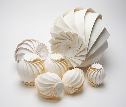
Recent Studies about Computer Aided Origami Design
J. Mitani, Univ. of Tsukuba
Origami is well known as the Japanese traditional art of folding paper. Today, origami is loved by all generations not only in Japan but also in the world. The manipulation of folding a square sheet of paper along a straight line has a deep relation to geometry. Origami has been the target of interest for mathematicians. The ridges and valleys appear when a sheet of paper is folded and unfolded again. We can obtain a lot of insights on origami by studying its pattern, called the crease pattern. Through the achievement of our predecessors, we now have plenty of knowledge about the geometry of origami. In 1980s, techniques for designing a crease pattern for making intended form were investigated, and they spread widely. As the results, amazingly realistic and complicated origami pieces, such as insects, animals, dinosaurs and so on, had been created. Since the computers had become popular, some software for designing origami appeared on the Web. We can say that the new era of origami has begun. One of remaining challenges is designing curved-origami which has curved folds. In this talk, recent studies about computer aided origami design and some interesting topics about origami will be presented.
*To register for the Luncheon Talk please refer to the registration
form for fee information. |
| Session 11A |
RTN [Shunju I] |
| Chairpersons |
R. Yamada, Hitachi Ltd.
R. Jammy, Sematech |
14:20 |
11A-1 |
Comprehensive Understanding of Random Telegraph
Noise with Physics Based Simulation |
| abstract |
Y. Higashi, N.
Momo, H.S. Momose, T. Ohguro and K. Matsuzawa |
| Toshiba
Corporation, Japan |
14:45 |
11A-2 |
Direct Real-Time Observation of Channel Potential
Fluctuation Correlated to Random Telegraph Noise of
Drain Current Using Nanowire MOSFETs with Four-
Probe Terminals |
| abstract |
K. Ohmori*,**,***, W. Feng**,***, S.
Sato****, R. Hettiarachchi**,***, M. Sato**,***, T.
Matsuki**,***, K. Kakushima****, H. Iwai**** and K.
Yamada*,**,*** |
| *University of Tsukuba, **Waseda University,
***JST-CREST and ****Tokyo Institute of Technology, Japan |
15:10 |
11A-3 |
Impact of Random Telegraph Signaling Noise on SRAM
Stability |
| abstract |
S.O. Toh, T.-J.K. Liu and B. Nikolić |
| University of
California, Berkeley, USA |
15:35 |
11A-4 |
A New Approach of NAND Flash Cell Trap Analysis
Using RTN Characteristics |
| abstract |
D. Kang*, S. Lee*, H.-M. Park*,
D.-j. Lee*, J. Kim*, J. Seo*, C. Lee*, C. Song*, C.-S. Lee*, H.
Shin**, J. Song*, H. Lee*, J.-H. Choi* and Y.-H. Jun* |
| *Samsung
Electronics Co., Ltd. and **Seoul National Univ., Korea |
| Session 11B |
MRAM and NAND [Shunju II] |
| Chairpersons |
N. Kasai, Tohoku Univ.
T. Skotnicki, STMicroelectronics |
14:20 |
11B-1 |
Integration of 28nm MJT for 8~16Gb Level MRAM with
Full Investigation of Thermal Stability |
| abstract |
Y. Kim, S.C. Oh,
W.C. Lim, J.H. Kim, W.J. Kim, J.H. Jeong, H.J. Shin, K.W. Kim,
K.S. Kim, J.H. Park, S.H. Park, H. Kwon, K.H. Ah, J.E. Lee, S.O.
Park, S. Choi, H.K. Kang and C. Chung |
| Samsung Electronics Co.,
Ltd., Korea |
14:45 |
11B-2 |
Strain-Engineering for High-Performance STT-MRAM |
| abstract |
Y.
Iba, K. Tsunoda, Y.M. Lee, C. Yoshida, H. Noshiro, A. Takahashi,
Y. Yamazaki, M. Nakabayashi, A. Hatada, M. Aoki and T. Sugii |
| Low-power Electronics Association & Project (LEAP), Japan |
| 15:10 |
11B-3 |
CoFeB/MgO Based Perpendicular Magnetic Tunnel
Junctions with Stepped Structure for Symmetrizing
Different Retention Times of “0” and “1” Information |
| abstract |
K.
Miura*,**, S. Ikeda*, M. Yamanouchi*, H. Yamamoto**, K.
Mizunuma*, H.D. Gan*, J. Hayakawa**, R. Koizumi*, F.
Matsukura* and H. Ohno* |
| *Tohoku University and **Hitachi,
Ltd., Japan |
15:35 |
11B-4 |
Highly Reliable 26nm 64Gb MLC E2NAND (Embedded-
ECC & Enhanced-Efficiency) Flash Memory with MSP
(Memory Signal Processing) Controller |
| abstract |
H. Shim, S.-S. Lee,
B. Kim, N. Lee, D. Kim, H. Kim, B. Ahn, Y. Hwang, H. Lee, J.
Kim, Y. Lee, H. Lee, J. Lee, S. Chang, J. Yang, S. Park, S.
Aritome, S. Lee, K.-O. Ahn, G. Bae and Y. Yang |
| Hynix
Semiconductor Inc., Korea |
| Session 12 |
Design Enablement II [Shunju I] |
| Chairpersons |
H. Morimura, NTT Microsystem Integration Laboratories
J. Cheek, Freescale |
16:15 |
12-1 |
Non-Gaussian Distribution of SRAM Read Current and
Design Impact to Low Power Memory Using Voltage
Acceleration Method |
| abstract |
J. Wang, P. Liu, Y. Gao, P. Deshmukh,
S. Yang, Y. Chen, W. Sy, L. Ge, E. Terzioglu, M. Abu-Rahma, M.
Garg, S.S. Yoon, M. Han, M. Sani and G. Yeap |
| Qualcomm Inc,
USA |
16:40 |
12-2 |
Variability and Technology Aware SRAM Product Yield
Maximization |
| abstract |
P. Zuber, M. Miranda, M. Bardon, S. Cosemans,
P. Roussel, P. Dobrovolny, T. Chiarella, N. Horiguchi, A. Mercha,
T.Y. Hoffmann, D. Verkest and S. Biesemans |
| IMEC, Belgium |
17:05 |
12-3 |
An Ultra Low-Noise MOSFET Device with Improved SNR
for DCO-Type Applications |
| abstract |
P. Srinivasan, A. Tsao, N. Nayak
and A. Marshall |
| Texas Instruments, USA |
17:30 |
12-4 |
Bridging Design and Manufacture of Analog/Mixed-
Signal Circuits in Advanced CMOS |
| abstract |
J. Feng*, A.L.S. Loke**,
T.T. Wee**, C.O. Lackey**, L.A. Okada*, C.T. Schwan***, T.
Mantei***, J.H. Morgan***, M.M. Herden***, J.G. Cooper**, Z.-
Y. Wu*, J.-S. Goo*, X. Li*, A.B. Icel*, L.A. Bair**, D.M.
Fischette**, B.A. Doyle**, E.S. Fang**, B.M. Leary** and S.
Krishnan* |
| *GLOBALFOUNDRIES, **AMD, Inc., USA and
***GLOBALFOUNDRIES, Germany |
|